
SiC VDMOSFET structure with low specific on-resistance and manufacturing method thereof

A conductive channel and drain electrode technology, which is applied in semiconductor/solid-state device manufacturing, circuits, electrical components, etc., can solve the problems of large on-resistance, high on-resistance, and high density of states, and achieve consistent flow and reduce Crowding, the effect of reducing the resistance of the drift region

Inactive Publication Date: 2015-04-22
INST OF SEMICONDUCTORS - CHINESE ACAD OF SCI
View PDF3 Cites 10 Cited by
  • Summary
  • Abstract
  • Description
  • Claims
  • Application Information

AI Technical Summary

Problems solved by technology

But in terms of technology, due to SiC / SiO 2 The surface interface state density is very high, the characteristic on-resistance is large, and it has the JFET effect at the same time, resulting in high on-resistance, and due to the concentration of power lines at the corners of the p-n interface, avalanche breakdown is prone to occur

Method used


Image

  • SiC VDMOSFET structure with low specific on-resistance and manufacturing method thereof
  • SiC VDMOSFET structure with low specific on-resistance and manufacturing method thereof
  • SiC VDMOSFET structure with low specific on-resistance and manufacturing method thereof

Examples


Embodiment Construction

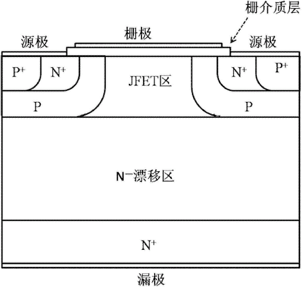
[0027] The total on-resistance of SiC VDMOSFET is composed of source contact resistance, source region resistance, inversion layer channel resistance, accumulation resistance, JFET resistance, drift region resistance, N + It is determined by substrate resistance and drain contact resistance. For a typical cell size, the inversion layer channel resistance, JFET resistance, and drift region resistance account for the vast majority of the total characteristic on-resistance.

[0028] In order to solve the foregoing technical problems, the conductive channel of the present invention uses an N-accumulation layer to replace the inversion layer, that is, an N - conductive channel layer.

[0029] figure 2 is a schematic diagram of the SiC VDMOSFET structure of the present invention. Such as figure 2 shown, the N - The conductive channel layer is formed between the gate dielectric layer and the P-type base region, and is connected to the N + source area and JFET area.

[0030] ...


PUM

PropertyMeasurementUnit
Thicknessaaaaaaaaaa
Doping concentrationaaaaaaaaaa

Abstract

The invention discloses a SiC VDMOSFET structure with low specific on-resistance and a manufacturing method of the SiC VDMOSFET structure with the low specific on-resistance. According to the structure, an N- drifting region is formed on an N+ substrate, a P-type base region and a JFET region are formed above the N- drifting region, and the P-type base region surrounds the JFET region; a P+ region and an N+ region are formed in the P-type base region; a gate dielectric layer is formed on the JFET region; an N- conductive channel layer is formed between the gate dielectric layer and the P-type base region and surrounds the JEFT region. An N current diffusion layer is formed on the joint of the JEFT region and the N- drifting region, and the width of the N current diffusion layer is the same as that of an N- drifting layer. Due to the SiC VDMOSFET structure, channel resistance and drifting region resistance can be lowered, and the on-resistance of the VDMOSFET structure can be lowered.

Description

technical field [0001] The invention belongs to the technical field of semiconductors, and in particular relates to a SiC VDMOSFET structure and a manufacturing method thereof which play an important role in the fields of high temperature, high frequency, medium and high voltage power electronics and the like. Background technique [0002] For a long time, Si materials have occupied a dominant position in the semiconductor field and are used in high-temperature and high-frequency circuits. However, with the advancement of technology and the expansion of application fields, Si-based devices are becoming more and more difficult to meet the requirements of harsher environments and higher performance, so people turn their attention to wide bandgap semiconductors. SiC material is considered to be a very potential third-generation semiconductor material. SiC material has higher breakdown field strength, higher carrier saturation velocity and higher thermal conductivity than Si mat...

Claims


Application Information

Patent Timeline
IPC IPC(8): H01L29/78H01L29/10H01L29/06H01L21/336
CPCH01L29/1033H01L29/66068H01L29/7802H01L29/1608H01L29/7828
Inventor 王进泽杨香颜伟刘胜北赵继聪何志王晓东杨富华
Owner INST OF SEMICONDUCTORS - CHINESE ACAD OF SCI
Learn More