H-shaped grid-control source-drain symmetrically-changeable tunneling transistor and manufacturing method thereof

A source-drain, symmetrical technology, applied in semiconductor/solid-state device manufacturing, diodes, semiconductor devices, etc., can solve the problems that the subthreshold swing of MOSFETs type devices cannot be reduced, and ordinary tunneling field effect transistors can only be used as one-way switches.

Active Publication Date: 2018-03-13
宿松新驱光电科技有限公司
View PDF2 Cites 0 Cited by
  • Summary
  • Abstract
  • Description
  • Claims
  • Application Information

AI Technical Summary

Problems solved by technology

[0004] In order to effectively combine and utilize the advantages of interchangeable source and drain of MOSFETs type devices and the low subthreshold swing swing of ordinary tunneling field effect transistors, solve the problem that the subthreshold swing of MOSFETs type devices cannot be reduced and ordinary tunneling field effect transistors It can only be used as a one-way switch. The present invention proposes an H-shaped gate-controlled source-drain symmetrical interchangeable tunneling transistor and its manufacturing method.

Method used


Image

  • H-shaped grid-control source-drain symmetrically-changeable tunneling transistor and manufacturing method thereof
  • H-shaped grid-control source-drain symmetrically-changeable tunneling transistor and manufacturing method thereof
  • H-shaped grid-control source-drain symmetrically-changeable tunneling transistor and manufacturing method thereof

Examples


Embodiment Construction

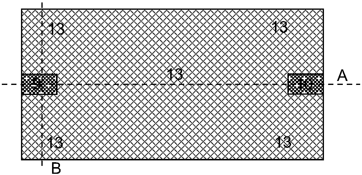
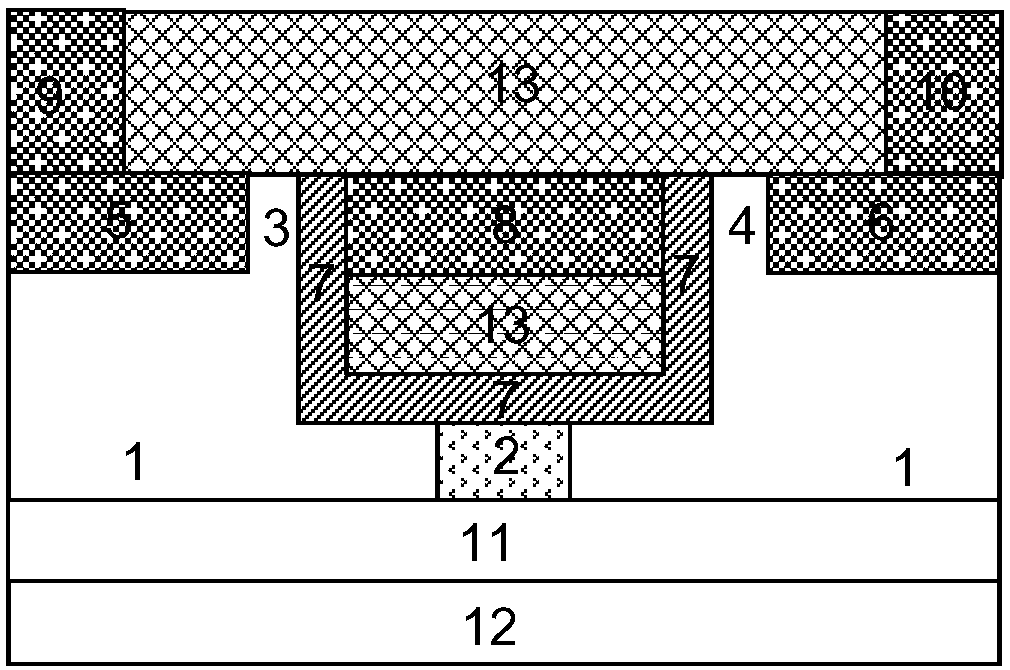
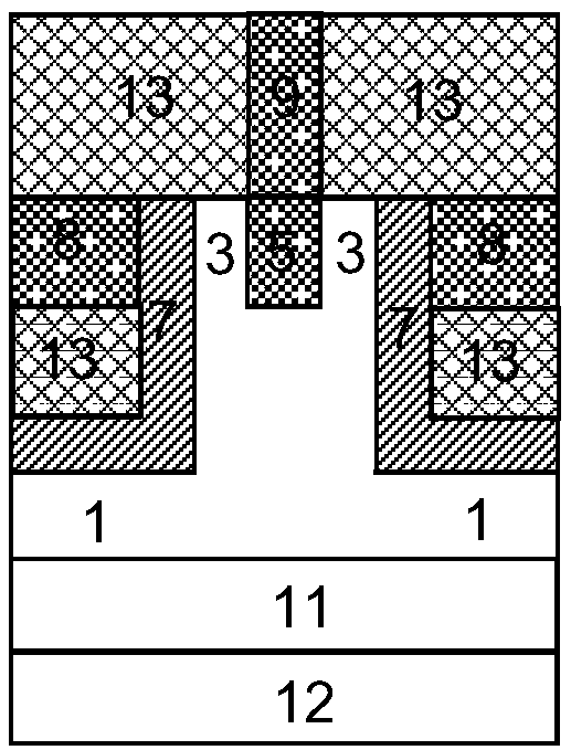
[0070] Below in conjunction with accompanying drawing, the present invention will be further described:

[0071] like figure 1 , figure 2 and image 3 As shown, an H-shaped gate-controlled source-drain symmetrical interchangeable tunneling transistor includes a silicon substrate 12 of an SOI wafer, and the silicon substrate 12 of the SOI wafer is above the substrate insulating layer 11 of the SOI wafer. Above the substrate insulating layer 11 of the SOI wafer is a single crystal silicon film 1 and a heavily doped region 2 of the first type of impurity; 16 cm -3 The single crystal silicon semiconductor material; the first type of impurity heavily doped region 2 is located in the middle region of the bottom horizontal part of the single crystal silicon thin film 1U-shaped structure, the conductivity type of the doped impurities determines the conduction type of the device, and its interior is not affected H-shaped gate electrode 8 field effect control, the impurity concentr...


PUM


Abstract

The invention relates to an H-shaped grid-control source-drain symmetrically-changeable tunneling transistor and a manufacturing method thereof. The device has characteristics of a rectangular grid and a horizontally-symmetric structure and has relatively high grid control capability, a second type of impurity heavily-doping source-drain changeable region can be controlled to be used as a source region or a drain region by adjusting a source-drain changeable electrode voltage, and the direction of a tunneling current is changed. The device has the advantages of low static power consumption, low reverse leakage current and low sub-threshold amplitude, and the bidirectional switch function can be achieved. Compared with a conventional MOSFETs device, the device has the advantages that more switch characteristic is achieved by a tunneling effect; and compared with a conventional tunneling field-effect transistor, the transistor has the bidirectional switch characteristic which a source and a drain are symmetric and can be changed with each other and which are not possessed by the conventional tunneling field-effect transistor, and thus, the transistor is suitable for promotion and application.

Description

technical field [0001] The invention relates to the field of ultra-large-scale integrated circuit manufacturing, in particular to an H-shaped gate-controlled source-drain symmetric interchangeable tunneling transistor with low leakage current suitable for low-power integrated circuit manufacturing and a manufacturing method thereof. Background technique [0002] According to the requirements of Moore's law, the basic unit MOSFETs of integrated circuits will become smaller and smaller in size, which will not only increase the difficulty of the manufacturing process, but also cause various adverse effects to become more prominent. Due to the limitation of the physical mechanism of current generation of MOSFETs used in integrated circuit design, the subthreshold swing cannot be lower than 60mV / dec. When the ordinary tunneling field effect transistor is used as a switching device, the tunneling effect of carriers between the semiconductor energy bands is used as the conduction m...

Claims


Application Information

Patent Timeline
Patent Type & Authority Applications(China)
IPC IPC(8): H01L29/739H01L21/331
CPCH01L29/66356H01L29/7391
Inventor 靳晓诗王艺澄刘溪
Owner 宿松新驱光电科技有限公司
Why Eureka
Try Eureka