Full-automatic intelligent-welding assembly line

A production line, fully automatic technology, applied in welding equipment, auxiliary equipment, metal processing, etc., can solve problems such as difficult quality assurance and low efficiency, and achieve the effects of reducing labor costs, accurate positioning, and improving product production efficiency and quality

Inactive Publication Date: 2015-04-29
OAEM TECH
View PDF11 Cites 13 Cited by
  • Summary
  • Abstract
  • Description
  • Claims
  • Application Information

AI Technical Summary

Problems solved by technology

[0002] With the development of society, there are more and more electronic products, and electronic products are closely related to our daily life. In the production process of electronic products, in the process of plug-in welding of electronic components, there will generally be defective solder joints, so it is necessary to inspect the PCB The board is inspected, and the solder joints of defective products are reprocessed to improve the yield rate. At present, many manufacturers use AOI devices to detect PCB boards. If there are bad solder joints, they will be marked. Then it is repaired manually; due to the high requirements of the soldering process of the PCB board, manual repair is used, the quality is difficult to guarantee, and the efficiency is low

Method used


Image

  • Full-automatic intelligent-welding assembly line

Examples


Embodiment

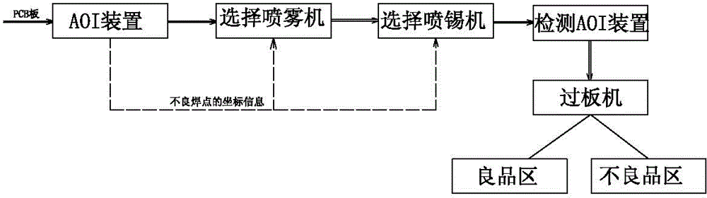
[0016] An intelligent welding automatic production line, including:

[0017] The AOI device is used to take pictures of the PCB board image and compare it with the good PCB board image, and calculate the coordinates of the bad solder points through software;

[0018] Choose a spray machine to spray flux on the bad solder joints on the PCB;

[0019] Select a soldering machine for correcting soldering of bad solder joints;

[0020] The transfer device is used to transfer the PCB board to the AOI device, the selective spray machine and the selective soldering machine in sequence.

[0021] During specific implementation, the transfer device sequentially transfers the PCB board to the AOI device, selects the sprayer, and selects the soldering machine. The transmission device first transmits the PCB board to the detection position of the AOI device. The AOI device takes pictures of the PCB board and compares it with the image of the good PCB board. The coordinates of the bad solde...


PUM


Abstract

The invention relates to the technical field of manufacture of PCB (printed circuit board) electron and power control boards, in particular to a full-automatic intelligent-welding assembly line. The full-automatic intelligent-welding assembly line comprises an AOI device, a selective mist sprayer, a selective soldering machine and a conveying device, wherein the AOI device is used for photographing PCBs to be compared with images of non-defective PCBs and calculating coordinates of defective soldering points through software; the selective mist sprayer is used for spraying soldering flux to the defective soldering points on the PCBs; the selective soldering machine is used for correcting soldering of the defective soldering points; the conveying device is used for sequentially conveying the PCBs to the AOI device, the selective mist sprayer and the selective soldering machine. The defective soldering points can be accurately positioned, the soldering flux and soldering tin can be sprayed one to one, maintenance and repair rate is high, production efficiency and quality of products are improved, and labor cost is reduced.

Description

technical field [0001] The invention relates to the technical field of PCB board production, in particular to an intelligent welding full-automatic production line. Background technique [0002] With the development of society, there are more and more electronic products, and electronic products are closely related to our daily life. In the production process of electronic products, in the process of plug-in welding of electronic components, there will generally be defective solder joints, so it is necessary to inspect the PCB The board is inspected, and the solder joints of defective products are reprocessed to improve the yield rate. At present, many manufacturers use AOI devices to detect PCB boards. If there are bad solder joints, they will be marked. Then it is repaired manually; due to the high requirements of the soldering process of the PCB board, manual repair is used, the quality is difficult to guarantee, and the efficiency is low. Contents of the invention [...

Claims


Application Information

Patent Timeline
Patent Type & Authority Applications(China)
IPC IPC(8): B23K3/00B23K3/08
CPCB23K3/00B23K3/082
Inventor 王庆富
Owner OAEM TECH
Why Eureka
Try Eureka