
Dynamic multi-selection-region division method based on FPGA (field programmable gate array) analytical layout solver
A technology for selecting regions and solvers, applied in complex mathematical operations, etc., can solve problems such as long processing time, bulky layout circuits, and failure to meet the requirements of program running time, achieving fast running speed and flexible division methods
- Summary
- Abstract
- Description
- Claims
- Application Information
AI Technical Summary
Problems solved by technology
Method used
Image

Examples
Embodiment Construction
[0025] The technical solutions of the present invention will be described in further detail below with reference to the accompanying drawings and embodiments.
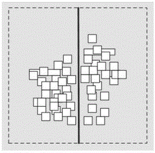
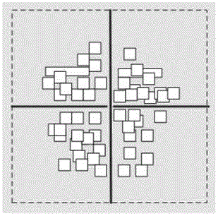
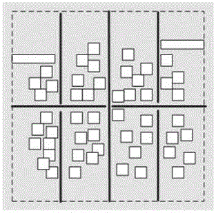
[0026] figure 1 It is a flow chart of a multi-choice area dynamic division method based on an FPGA analytical layout solver in an embodiment of the present invention. In the figure, the multi-choice area dynamic division method includes:
[0027] Step 101, convert user circuits into gate-level circuits, map the gate-level circuits into look-up tables and / or registers, combine the look-up tables and / or registers into LEs, and generate netlists.
[0028] figure 2 It is a flowchart of the layout algorithm of the embodiment of the present invention. Before implementing the layout algorithm, such as figure 2 In the flowchart of the layout algorithm of the present invention, in the stage of synthesis and library mapping, the user circuit needs to be converted into a gate-level circuit. The user circuit is compiled using...
PUM
 Abstract
Description
Claims
Application Information