Method and structure for improving inter-sheet uniformity of phosphorus concentration in doped polycrystalline or amorphous silicon

A technology of phosphorus concentration and amorphous silicon, which is applied in the field of improving the uniformity of doped polycrystalline or amorphous silicon phosphorus concentration between sheets, and improving the uniformity of doped polycrystalline or amorphous silicon phosphorus concentration between sheets, can solve the problem of Problems such as multiple particles and high cost, to achieve uniform distribution of phosphorus concentration, reduce production costs, and improve the uniformity of phosphorus concentration

Active Publication Date: 2019-06-11
SHANGHAI HUAHONG GRACE SEMICON MFG CORP
View PDF3 Cites 0 Cited by
  • Summary
  • Abstract
  • Description
  • Claims
  • Application Information

AI Technical Summary

Problems solved by technology

Therefore, in the prior art, in order to ensure that the phosphorus concentration of the product on the entire wafer boat or the entire batch of products is still within the product demand range, the general method is to greatly increase the flow rate of the reaction gas silane, but this method will cause multiple particles and cost (cost) ) becomes a higher production problem

Method used


Image

  • Method and structure for improving inter-sheet uniformity of phosphorus concentration in doped polycrystalline or amorphous silicon
  • Method and structure for improving inter-sheet uniformity of phosphorus concentration in doped polycrystalline or amorphous silicon
  • Method and structure for improving inter-sheet uniformity of phosphorus concentration in doped polycrystalline or amorphous silicon

Examples


Embodiment Construction

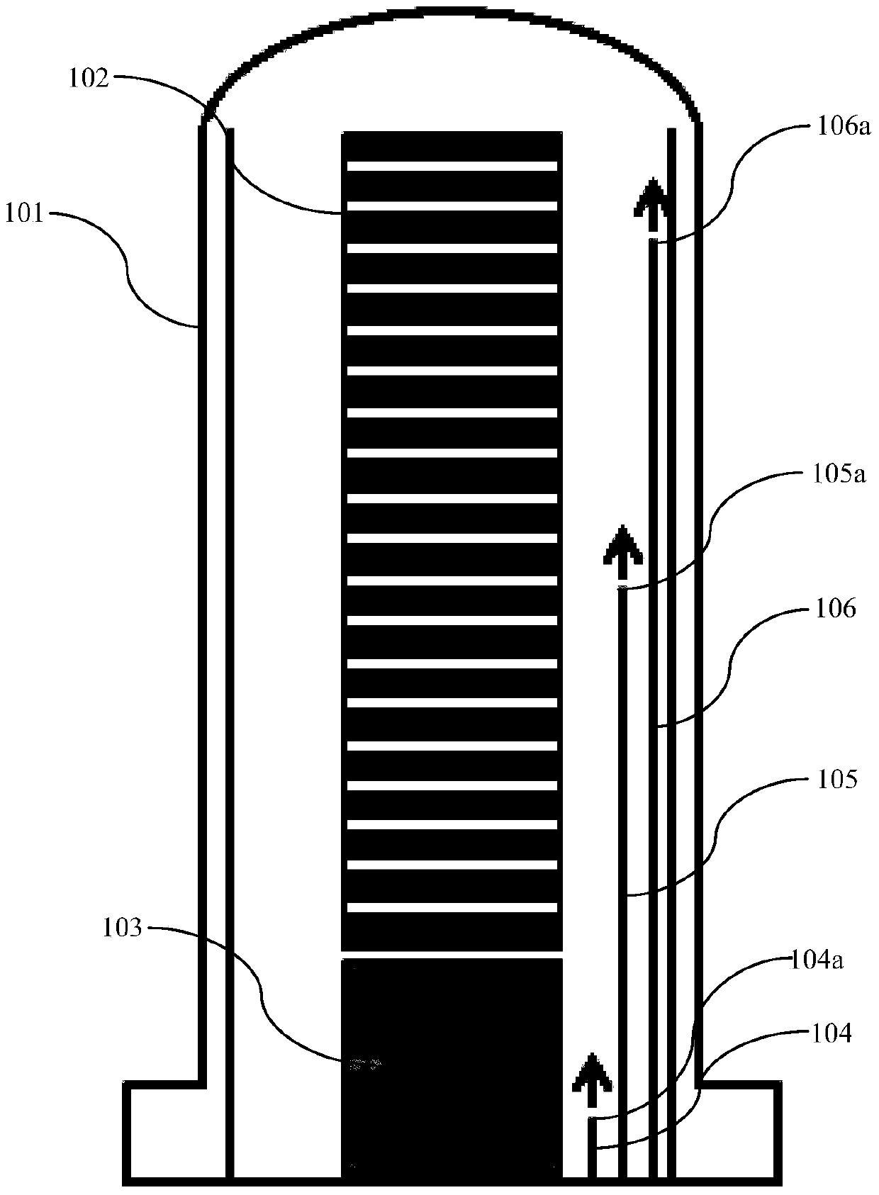
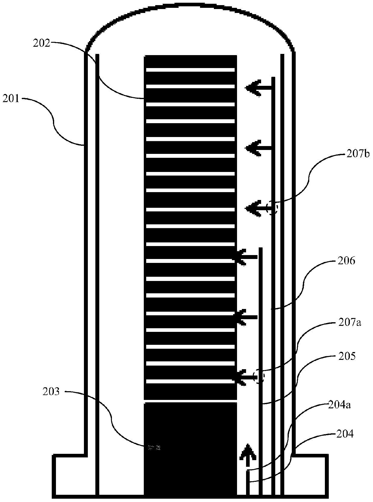
[0053] Such as image 3 Shown is a schematic structural view of the furnace tube 201 of the embodiment of the present invention; the embodiment of the present invention improves the uniformity of doped polycrystalline or amorphous silicon phosphorus concentration between sheets using the furnace tube 201 to grow polycrystalline silicon or amorphous silicon and simultaneously For phosphorus doping, a crystal boat 202 is arranged in the cavity of the furnace tube 201 , and the crystal boat 202 is placed on a heat preservation bucket 203 . The crystal boat 202 is used to place silicon wafers for growing polysilicon or amorphous silicon. Phosphine is used as a gas source for phosphorus doping, and the phosphine is passed into the cavity of the furnace tube 201 through a 3-way nozzle pipeline. In the body, the top of the first nozzle pipeline 204 is arranged on the bottom of the wafer boat 202, the top of the second nozzle pipeline 205 is arranged in the middle of the wafer boat 20...


PUM

PropertyMeasurementUnit
pore sizeaaaaaaaaaa
lengthaaaaaaaaaa
lengthaaaaaaaaaa

Abstract

The invention discloses a method for improving the phosphorus concentration uniformity of doped polycrystalline or noncrystalline silicon chips. According to the method, a furnace tube is adopted for growth, phosphorane is introduced through three nozzle pipelines, and the top ends of the nozzle pipelines are arranged at the bottom, the middle and the top of a crystal boat respectively; gas is emitted from the top of the first nozzle pipeline; a plurality of lateral gas outlets are formed in each of the second and third nozzle pipelines at intervals; the diameters of the lateral gas outlets of each pipeline are gradually increased in a direction from the bottom end to the top end and adjusted by testing the phosphorus concentration of the monitored silicon chips at the fixed monitoring positions of the crystal boat; the positions of the lateral gas outlets are adjusted by testing a phosphorus concentration curve along the whole crystal boat. The invention further discloses a structure for improving the phosphorus concentration uniformity of the doped polycrystalline or noncrystalline silicon chips. According to the method and the structure, the phosphorus concentration uniformity of the silicon chips can be improved and the production cost can be reduced.

Description

technical field [0001] The invention relates to the field of semiconductor integrated circuit manufacturing, in particular to a method for improving the uniformity of doped polycrystalline or amorphous silicon phosphorus concentration between sheets, and the invention also relates to a method for improving the doped polycrystalline or amorphous silicon phosphorus concentration sheet Uniform structure. Background technique [0002] Doped polysilicon / amorphous silicon, that is, the phosphorus concentration of the polysilicon or amorphous silicon process directly affects the gate resistance (Rg) parameter of the product, which is a very critical and controllable process parameter. Existing polysilicon or amorphous silicon is generally grown by a furnace tube process and simultaneously doped. In the growth process of polysilicon or amorphous silicon, silane is generally used as the silicon source, and phosphine is used as the doping source of phosphorus. Due to the equipment se...

Claims


Application Information

Patent Timeline
Patent Type & Authority Patents(China)
IPC IPC(8): H01L21/223C30B31/16
Inventor 侯翔宇周利明朱晓斌
Owner SHANGHAI HUAHONG GRACE SEMICON MFG CORP
Why Eureka
Try Eureka