Light emitting diode structure

A technology of light-emitting diodes and electrodes, applied to electrical components, circuits, semiconductor devices, etc., can solve the problems of low light reflectivity, limited light extraction efficiency, low reflectivity, etc., achieve high reflectivity, improve reflectivity, and increase reflection The effect of the angle

Active Publication Date: 2015-04-29
XIAMEN CHANGELIGHT CO LTD
View PDF6 Cites 2 Cited by
  • Summary
  • Abstract
  • Description
  • Claims
  • Application Information

AI Technical Summary

Problems solved by technology

The traditional DBR structure only has a strong reflection effect on light incident at vertical and small angles, but the reflectivity of light incident at large angles is very low, which greatly limits the light extraction efficiency of LEDs.
[0005] In view of the defect of the light-emitting diode DBR in the prior art that the light reflectance emitted by the active region is low, the inventor proposed a light-emitting diode structure that overcomes the defect, and this case arose from this

Method used


Image

  • Light emitting diode structure
  • Light emitting diode structure
  • Light emitting diode structure

Examples


Embodiment Construction

[0034] The present invention will be described in detail below in conjunction with the accompanying drawings and specific embodiments.

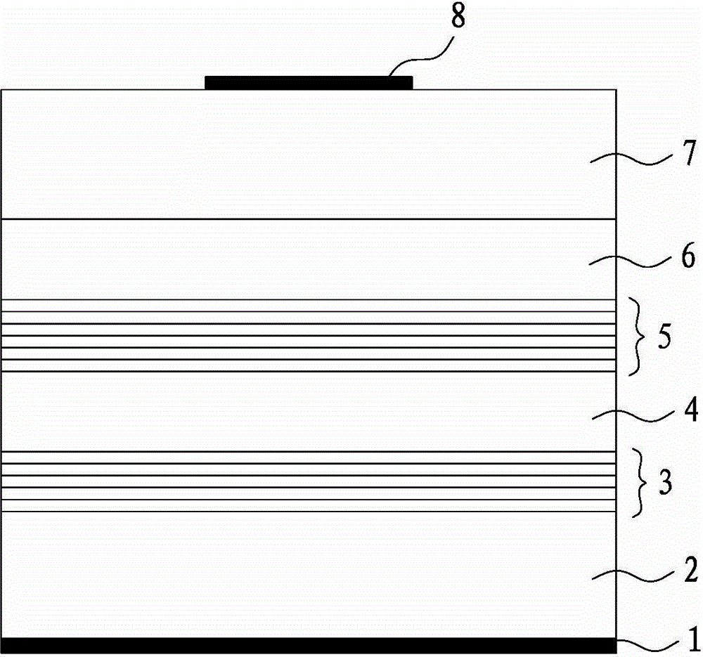
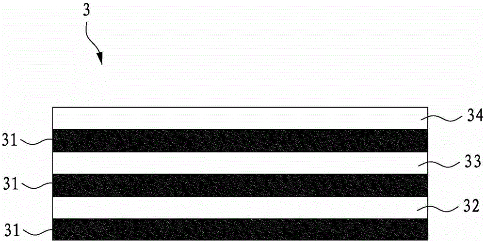
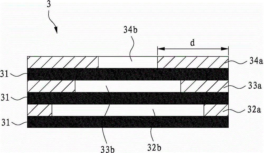
[0035] The invention discloses a light-emitting diode structure. A substrate is provided. There is a first electrode on the lower surface of the substrate, and a DBR reflective layer, a first-type confinement layer, an active layer, and a second-type confinement layer are sequentially distributed on the upper surface of the substrate. The confinement layer and the current spreading layer; the second electrode is formed on the current spreading layer; the low refractive index layer in the DBR reflective layer is partially oxidized, and the oxidation conditions are: the temperature is 300-600°C, and the oxidation is under the condition of water vapor; and The oxidation depth of each low refractive index layer changes gradually or periodically from bottom to top in the normal direction of the DBR reflective layer.

[0036] The DBR reflective lay...


PUM


Abstract

The invention discloses a light emitting diode structure. A substrate is provided; a first electrode is arranged on the lower surface of the substrate; a DBR reflecting layer, a first type limiting layer, an active layer, a second type limiting layer and a current expanding layer are distributed on the upper surface of the substrate in sequence; a second electrode is formed on the current expanding layer; low refractive index layers in the DBR reflecting layer are locally oxidized, and the oxidation depths of the low refractive index layers gradually change or periodically change from bottom to top in the normal direction of the DBR reflecting layer. The oxidation depths of oxidizing layers gradually change or periodically change, and lights emitting into a DBR are bent, so that the reflecting angle of the DBR is increased, the reflectivity of the DBR is increased, and the brightness of a chip is improved.

Description

technical field [0001] The invention relates to a light emitting diode structure. Background technique [0002] Light-emitting diodes are widely used in the fields of display, indication and lighting due to their high efficiency, energy saving and environmental protection. The common substrate of AlGaInP (aluminum indium gallium phosphide) light-emitting diodes is GaAs (gallium arsenide), and its absorption limit is about 870nm. Therefore, some of the light emitted by AlGaInP light-emitting diodes will be absorbed by the GaAs substrate. [0003] In the prior art, in order to prevent the light incident on the GaAs substrate from being absorbed by the substrate, a Bragg reflective layer (DBR) is often inserted between the active layer of the LED and the substrate, and the Bragg reflective layer is usually composed of a complex array The high-refractive-index layer and the low-refractive-index layer are alternately arranged to reflect the light incident on the substrate and em...

Claims


Application Information

Patent Timeline
IPC IPC(8): H01L33/10
CPCH01L33/10H01L33/30
Inventor 陈凯轩林志伟李涛彭绍文
Owner XIAMEN CHANGELIGHT CO LTD
Why Eureka
Try Eureka