Inductor layout, and voltage-controlled oscillator (VCO) system

An inductance and layout technology, applied in the field of inductance layout, can solve the problems of increased manufacturing cost, increased integrated circuit area, increased integrated circuit silicon area, etc., to achieve the effect of increasing the tuning range

Active Publication Date: 2015-04-29
TELEFON AB LM ERICSSON (PUBL)
View PDF8 Cites 45 Cited by
  • Summary
  • Abstract
  • Description
  • Claims
  • Application Information

AI Technical Summary

Problems solved by technology

The use of inductive switching or dual-mode transformer type resonators is associated with a degradation in phase noise performance due to the unavoidable introduction of additional losses in the resonator circuit
[0005] Alternative phase-locked loop (PLL) schemes using local oscillator (LO) dividers with division ratios other than multiples of 2, which reduce the required VCO tuning range , but they exhibit some undesirable properties in terms of waveform duty cycle, quadrature signal output availability, IQ phase accuracy, etc.
[0006] Using multiple VCOs to cover the required frequency range is a straightforward and flexible solution, with the obvious disadvantage of increasing the silicon area of ​​these parts of the integrated circuit containing the VCOs
Therefore, the disadvantage of multiple VCOs is that it requires an increased integrated circuit area compared to a single VCO solution
This is especially a disadvantage due to the trend towards smaller and smaller integrated circuits to fit into ever smaller electronic devices
also incurs an increase in manufacturing cost directly related to the total die area of ​​the integrated circuit

Method used


Image

  • Inductor layout, and voltage-controlled oscillator (VCO) system
  • Inductor layout, and voltage-controlled oscillator (VCO) system
  • Inductor layout, and voltage-controlled oscillator (VCO) system

Examples


Embodiment Construction

[0027] Here the invention will be explained by the following non-limiting description.

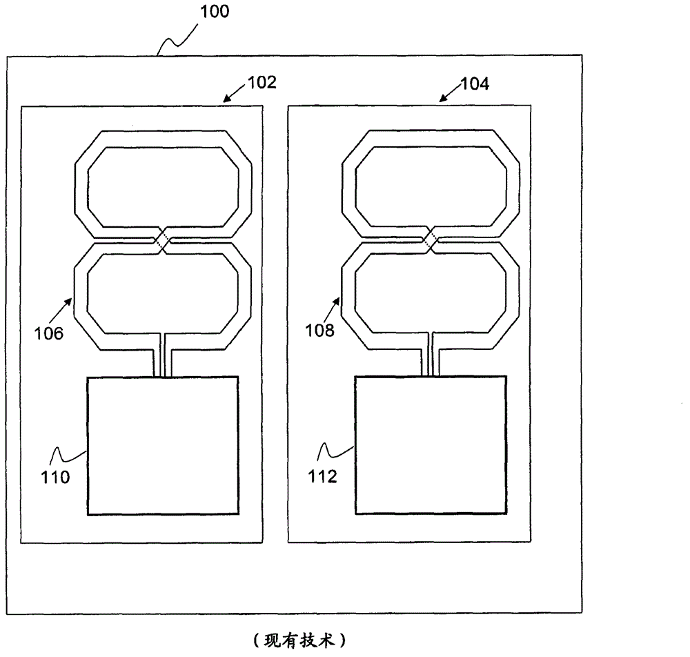
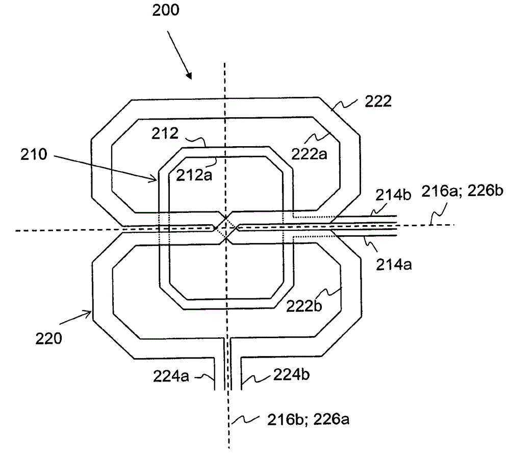
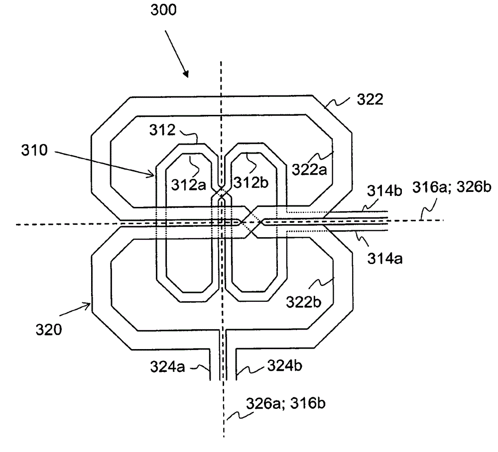
[0028] figure 2 , 3 and 4 schematically show embodiments of inductor layouts 200 , 300 , 400 . The embodiments of the inductor layout 200, 300, 400 are compared with the inductor layout using the same area size in the prior art, relative to the integrated circuit ( figure 2 -4 not shown), provides an increased frequency tuning range.

[0029] The inductance layout 200 , 300 , 400 comprises a first inductance 210 , 310 , 410 and a second inductance 220 , 320 , 420 . The first and second inductances 210, 310, 410; 220, 320, 420 are electrically and magnetically independent inductances.

[0030] The expression "electrically and magnetically independent inductance" means that these inductances have a very small electromagnetic coupling coefficient k, usually much smaller than 0.1. Therefore, the first and second inductances 210, 310, 410; 220, 320, 420 as independent inductances exhibit...


PUM


Abstract

An inductor layout 200,300,400 comprising a first inductor 210,310,410 and a second inductor 220,320,420. The first and second inductors 210,310,410; 220,320,420 are electrically and magnetically independent inductors concentrically arranged on an integrated circuit 800. At least one of the first and second inductors 210, 310,410; 220,320,420 is a multi-loop inductor with a first axis 226a,316a,326a,416a,426a of symmetry.

Description

technical field [0001] Embodiments herein relate to inductive layouts, voltage controlled oscillator (VCO) systems, integrated circuit subsystems, integrated radio frequency (RF) transceiver circuits, communication devices, and applications of inductive layouts in integrated circuits. In particular, embodiments relate to frequency modulation in integrated circuits. Background technique [0002] In the future, integrated RF transceiver circuits used in cellular communication devices will have to handle an increasing number of cellular standards and associated frequency bands. Requirements regarding the frequency tuning range of a voltage controlled oscillator (VCO) in a local oscillator (LO) signal generation subsystem are becoming increasingly difficult while maintaining acceptable performance in other key performance metrics such as phase noise, current consumption, etc. satisfy. [0003] The trend toward single-chip solutions, also known as "system-on-chip" solutions, ha...

Claims


Application Information

Patent Timeline
Patent Type & Authority Applications(China)
IPC IPC(8): H01F17/00
CPCH01L28/10H01F17/0006H01F27/2804H01F27/346H01F2017/0073H03B5/02H03B5/12H03B2201/0216H04B1/40
Inventor T·马特斯森P·安德里尼
Owner TELEFON AB LM ERICSSON (PUBL)
Why Eureka
Try Eureka