

Design method of memory anti-multi-bit flip reliability evaluation model under the influence of negative bias temperature instability
A technology of negative bias temperature and instability, applied in static memory, instruments, etc., can solve the problem of low accuracy of model evaluation, and achieve the effect of improving accuracy
- Summary
- Abstract
- Description
- Claims
- Application Information
AI Technical Summary
Problems solved by technology
Method used
Image

Examples
specific Embodiment approach 1
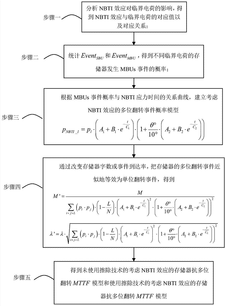
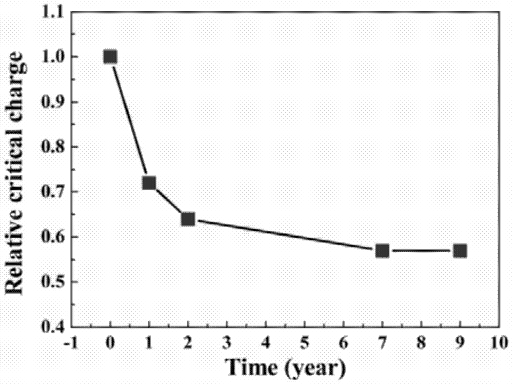
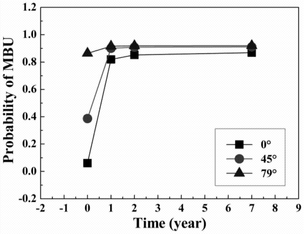
[0048] Specific implementation mode one: combine figure 1 Describe this embodiment, the design method of the memory anti-multi-bit flip reliability evaluation model under the influence of negative bias temperature instability,
[0049] Realized based on the following assumptions:
[0050] (1) The soft errors in the memory conform to the Poisson distribution;
[0051] (2) The probability of soft errors in the storage unit is uniformly distributed;
[0052] (3) At least two radiation events are required for the failure of the memory; when using ECC hardening technology, if the maximum number of error bits caused by an MBUs event in the memory is L, the ECC with the correction capability of L will be used; only when there are more than one word When an error occurs in the L bit, the memory will fail once;
[0053] (4) Two radiation events on a word are the main factors of memory failure; since the correction capability of ECC is the same as the maximum number of errors on a wo...
specific Embodiment approach 2
[0089] Specific embodiment two: formula (10) (11) described in this embodiment and effective boundary condition of formula (14) are respectively:
[0090]
[0091]
[0092] Among them, β is the probability that two radiation events produce more flipping digits than L; β nonscrubbing is β without erasing technique, β scrubbing is β using the erasure technique.
[0093] Other steps are the same as in the first embodiment.
specific Embodiment approach 3
[0094] Specific Embodiment Three: The memory described in this embodiment is a memory manufactured by a CMOS process below 65nm.
[0095] Other steps are the same as in the second embodiment.
PUM
 Abstract
Description
Claims
Application Information