TSV (through silicon via) back side hole leaking technology without CMP (chemical mechanical grinding) technology

A technology for through silicon vias and processes, applied in the field of through-silicon via backside leakage process solutions, can solve the problems of complex process, high cost, low production capacity, etc., and achieve the effects of avoiding CMP process, improving output efficiency and reducing process cost.

Inactive Publication Date: 2015-05-20
NAT CENT FOR ADVANCED PACKAGING
View PDF5 Cites 5 Cited by
  • Summary
  • Abstract
  • Description
  • Claims
  • Application Information

AI Technical Summary

Problems solved by technology

However, the CMP process has problems such as comp

Method used


Image

  • TSV (through silicon via) back side hole leaking technology without CMP (chemical mechanical grinding) technology
  • TSV (through silicon via) back side hole leaking technology without CMP (chemical mechanical grinding) technology
  • TSV (through silicon via) back side hole leaking technology without CMP (chemical mechanical grinding) technology

Examples


Embodiment Construction

[0027] The present invention will be further described below in conjunction with specific drawings and embodiments.

[0028] The TSV back leakage process scheme proposed in this embodiment without CMP process includes the following steps:

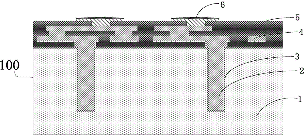
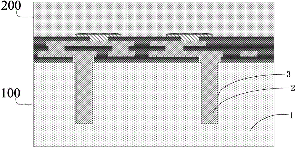
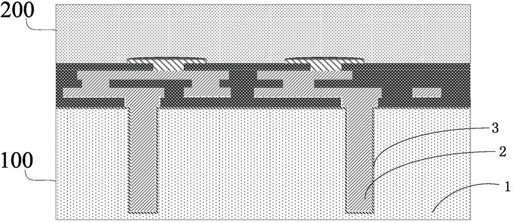
[0029] S1. Provide a device wafer 100 that has completed the front process; figure 1 As shown, the device wafer 100 has completed the fabrication of the front structure according to the existing conventional process; the device wafer 100 includes a substrate 1, a TSV blind hole 2 in the substrate 1, an insulating layer and a seed on the wall of the TSV blind hole 2 layer (the two layers are marked with a mark 3), the front RDL layer 4, the front dielectric layer 6 and the connection bump 6 connecting the front RDL layer, etc.; the TSV blind hole 2 is filled with conductive metal, such as copper.

[0030] The substrate 1 is a silicon substrate. The TSV hole is a through-silicon hole. In step S1, since the TSV hole has not realized the expo...


PUM


Abstract

The invention provides a TSV (through silicon via) back side hole leaking technology without CMP (chemical mechanical grinding) technology. The TSV back side hole leaking technology comprises the following steps of S1, providing a device wafer which completes a front side technology, wherein the device wafer comprises a substrate and a TSV (through silicon via) blind hole, and the TVS blind hole is formed in the substrate; S2, providing a carrier wafer, and bonding the front side of the device wafer and the carrier wafer by a temporary bonding technology, so as to obtain a temporary bonding body; S3, mechanically grinding the back side of the substrate of the device wafer, and thinning; S4, etching the back side of the substrate, and enabling the TSV blind hole to expose out of the back side of the substrate; S5, coating a back side medium layer at the back side of the substrate of the device wafer, and completely covering the exposing part of the TSV blind hole in the step S4; S6, utilizing a mechanical grinding technology to process the back side medium layer, and enabling the TSV blind hole to expose out of the back side medium layer. The TSV back side hole leaking technology has the advantages that the CMP process in the TSV back side end exposing process is avoided, the technological cost is greatly reduced, the output efficiency is obviously improved, and the self-aligning effect of the back side medium layer hole via is realized.

Description

technical field [0001] The invention relates to a wafer packaging process, in particular to a back leakage hole process scheme of a through-silicon hole replacing a CMP process. Background technique [0002] With the development of people's requirements for electronic products in the direction of miniaturization, multi-function, and environmental protection, people strive to make electronic systems smaller and smaller, with higher integration and more functions. , due to the high packaging density of 2.5D packaging and 3D packaging, it has attracted extensive attention. [0003] In 2.5D packaging, the bonding of the carrier wafer and the device wafer is achieved using temporary bonding technology. Temporary bonding has the following advantages: First, the carrier wafer provides mechanical support and protection for the thin device wafer so that backside processing can be performed with standard device fab equipment. For ultra-thin device wafers, process processing at the d...

Claims


Application Information

Patent Timeline
IPC IPC(8): H01L21/768
CPCH01L21/76898
Inventor 薛恺李昭强张文奇
Owner NAT CENT FOR ADVANCED PACKAGING
Why Eureka
Try Eureka