Manufacturing method of oxide semiconductor thin film transistor array substrate

A technology of oxide semiconductors and thin film transistors, which is applied in semiconductor/solid-state device manufacturing, semiconductor devices, and photolithography on patterned surfaces, etc. It can solve problems such as rising production costs and complex manufacturing processes, and achieve improved performance and low process temperature. , The effect of streamlining the process

Active Publication Date: 2017-12-15
KUSN INFOVISION OPTOELECTRONICS
View PDF4 Cites 0 Cited by
  • Summary
  • Abstract
  • Description
  • Claims
  • Application Information

AI Technical Summary

Problems solved by technology

[0005] While the display performance of the prior art liquid crystal display is improved, the disadvantage is that it will require more masks and more complicated manufacturing processes during production, which will increase the production cost.

Method used


Image

  • Manufacturing method of oxide semiconductor thin film transistor array substrate
  • Manufacturing method of oxide semiconductor thin film transistor array substrate
  • Manufacturing method of oxide semiconductor thin film transistor array substrate

Examples


no. 1 example

[0045] Figure 1 to Figure 8 It is a schematic cross-sectional view of the manufacturing process of the oxide semiconductor thin film transistor array substrate in the first embodiment of the present invention, and the manufacturing method includes:

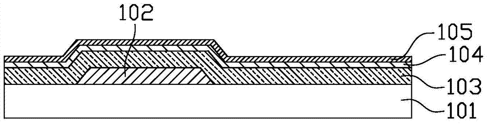
[0046] Such as figure 1 As shown, firstly, a gate 102 is formed on a base substrate 101 . Specifically, the base substrate 101 is, for example, a transparent glass substrate, and the gate 102 can be fabricated and formed on the base substrate 101 through a photolithography process. The photolithography process mainly includes film layer deposition, photoresist coating, exposure, development, and etching. , Photoresist removal and other processes are well known to those skilled in the art and will not be repeated here.

[0047] Such as figure 1 As shown, a gate insulating layer 103 , an oxide semiconductor layer 104 , and a pixel electrode layer 105 are sequentially deposited on the gate 102 to form. The material of the gate ...

no. 2 example

[0071] Figure 9 to Figure 11 It is the second embodiment of the present invention, which differs from the first embodiment in that its TFT device adopts an etch barrier structure, that is, the oxide semiconductor layer 104 and the source electrode in the active layer region 201 are compared with the first embodiment. 111 . An etch stopper layer (ESL) 115 is added between the drain electrodes 112 to protect the semiconductor channel of the active layer from being damaged by the etching process of the source-drain metal layer. The process before forming the etching stopper layer 115 in this embodiment is common to that of the first embodiment, please refer to the description of the corresponding process in the first embodiment and Figure 1 to Figure 6 .

[0072] Before the etching stopper layer 115 is formed, it is preferable to perform etching damage repair treatment on the oxide semiconductor layer 104 as the active layer, such as adding O2 plasma treatment, N2O plasma trea...

no. 3 example

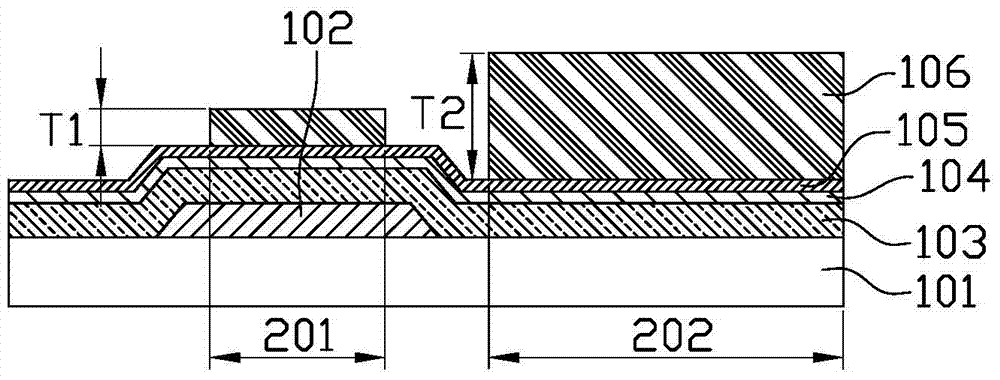
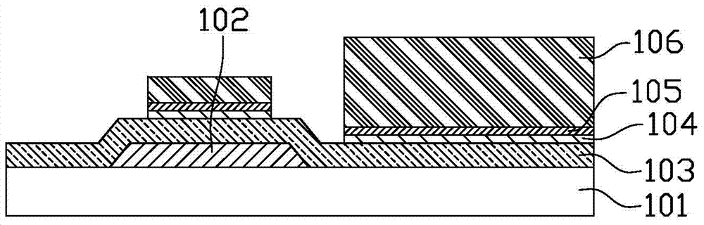
[0079] Figure 12 to Figure 18 It is the third embodiment of the present invention, which differs from the first embodiment in the half-exposure process of the photoresist 106 coated on the pixel electrode layer 105 and the structure on the active layer.

[0080] Such as Figure 12 As shown, when the photoresist 106 is half-exposed, the half-exposed area is changed from the entire active layer area 201 to the TFT back channel area, that is, only the TFT back channel area is half-exposed, which is equivalent to reducing the half-exposure area. In other words, the active layer region 201 can be divided into three sub-regions: the middle, the left and the right. The middle region corresponds to the TFT back channel region. In this embodiment, only the active layer region 201 located in the middle The photoresist 106 on the active layer region 201 is half-exposed, and the photoresist 106 on both sides (left and right) of the active layer region 201 is normally exposed (fully exp...


PUM


Abstract

The invention relates to a method for manufacturing an oxide semiconductor thin film transistor array substrate. The method comprises the following steps of manufacturing a grid on a lining substrate; sequentially depositing on the grid to form a grid insulation layer, an oxide semiconductor layer and a pixel electrode layer; coating a photoresist on the pixel electrode layer, performing half exposure on a photoresist on an active source area, and enabling the thickness of the photoresist on the active source area to be smaller than the thickness of the photoresist on the pixel electrode area; etching to remove the pixel electrode layer and the oxide semiconductor layer outside the active layer area and the pixel electrode area; removing the photoresist on the active source layer; etching to remove the pixel electrode layer on the oxide semiconductor layer in the active layer area, and exposing the oxide semiconductor layer in the active layer area; removing the photoresist on the pixel electrode area; manufacturing a source and a drain on the oxide semiconductor layer in the active layer area; manufacturing a protecting layer on the source and the drain; manufacturing a common electrode layer on the protecting layer.

Description

technical field [0001] The invention relates to the field of display technology, in particular to a method for manufacturing an oxide semiconductor thin film transistor array substrate. Background technique [0002] Due to the low electron mobility of amorphous silicon (a-Si) due to its own defects, its application in the display field is limited. Oxide semiconductor thin film transistor (OS-TFT) refers to a thin film transistor whose semiconductor channel is made of oxide semiconductor. Oxide semiconductor has the characteristics of high electron mobility, low process temperature and high light transmittance. Therefore, it has become one of the research hotspots in the field of thin film transistor display. [0003] Liquid crystal display has the advantages of good picture quality, small size, light weight, low driving voltage, low power consumption, no radiation and relatively low manufacturing cost. It currently dominates the field of flat panel display, and with the rap...

Claims


Application Information

Patent Timeline
Patent Type & Authority Patents(China)
IPC IPC(8): H01L21/77G03F7/00
CPCH01L27/1225H01L27/1288
Inventor 何佳新
Owner KUSN INFOVISION OPTOELECTRONICS
Why Eureka
Try Eureka