

High photoresponse near-infrared photodetector
A near-infrared optical and electrical detector technology, applied in the direction of circuits, electrical components, semiconductor devices, etc., can solve the problem of light response, poor thermal conductivity and mechanical properties of antimony selenide thin film photodetectors, and dark quantum efficiency of detectors. Low current and other problems, to achieve the effect of abundant reserves, low price, and easy control of process parameters
- Summary
- Abstract
- Description
- Claims
- Application Information
AI Technical Summary
Problems solved by technology
Method used
Image

Examples
Embodiment 1
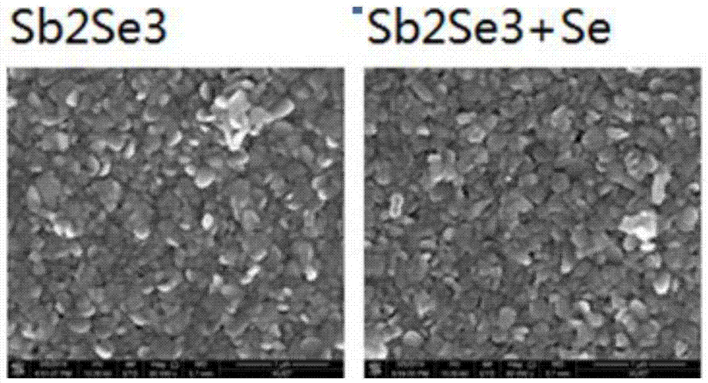
[0024] A near-infrared photodetector with high light response, the specific structure is a transparent inert substrate / antimony selenide thin film / electrode, wherein the antimony selenide thin film is obtained by post-selenization treatment;
[0025] Its concrete preparation steps are as follows:
[0026] Step 1: Cleaning the substrate: Clean the transparent inert substrate white glass with deionized water, acetone, isopropanol, and deionized water for 16 minutes each, and then blow dry with a nitrogen gun;
[0027] Step 2: Deposit an antimony selenide thin film on the surface of the transparent and inert substrate white glass described in step 1 by thermal evaporation, the evaporation source temperature is 330°C, the substrate heating temperature is 290°C, and the evaporation time is 40min, the deposited selenium Antimony film thickness is 500nm;
[0028] Step 3: annealing the antimony selenide thin film described in step 2 in a selenium atmosphere, the selenium atmosphere i...
Embodiment 2
[0031] A near-infrared photodetector with high light response, the specific structure is a transparent inert substrate / antimony selenide thin film / electrode, wherein the antimony selenide thin film is obtained by post-selenization treatment;
[0032] Its concrete preparation steps are as follows:
[0033] Step 1: Clean the substrate: Clean the transparent inert substrate ceramic sheet with deionized water, acetone, isopropanol, and deionized water for 16 minutes each, and then blow dry with a nitrogen gun;
[0034] Step 2: Deposit an antimony selenide thin film on the surface of the transparent inert substrate ceramic sheet described in step 1 by thermal evaporation, the evaporation source temperature is 330°C, the substrate heating temperature is 290°C, and the evaporation time is 40min, the deposited selenium Antimony film thickness is 500nm;
[0035]Step 3: Deposit a layer of selenium on the surface of the antimony selenide film described in step 2, wherein the evaporation...
PUM
| Property | Measurement | Unit |
|---|---|---|
| thickness | aaaaa | aaaaa |
Abstract
Description
Claims
Application Information