

Array substrate and manufacturing method thereof
A technology for array substrates and manufacturing methods, which is applied in the field of array substrates and array substrate manufacturing, and can solve the problems of reduced aperture ratio, too small capacitance, and reduced aperture ratio, etc.
- Summary
- Abstract
- Description
- Claims
- Application Information
AI Technical Summary
Problems solved by technology
Method used
Image

Examples
Embodiment Construction
[0049] In order to understand the above-mentioned purpose, features and advantages of the present invention more clearly, the present invention will be further described in detail below in conjunction with the accompanying drawings and specific embodiments. It should be noted that, in the case of no conflict, the embodiments of the present application and the features in the embodiments can be combined with each other.
[0050] In the following description, many specific details are set forth in order to fully understand the present invention. However, the present invention can also be implemented in other ways different from those described here. Therefore, the protection scope of the present invention is not limited by the specific details disclosed below. EXAMPLE LIMITATIONS.
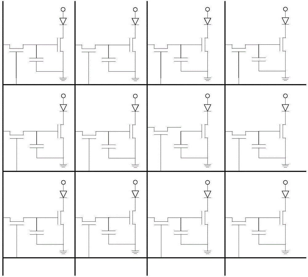
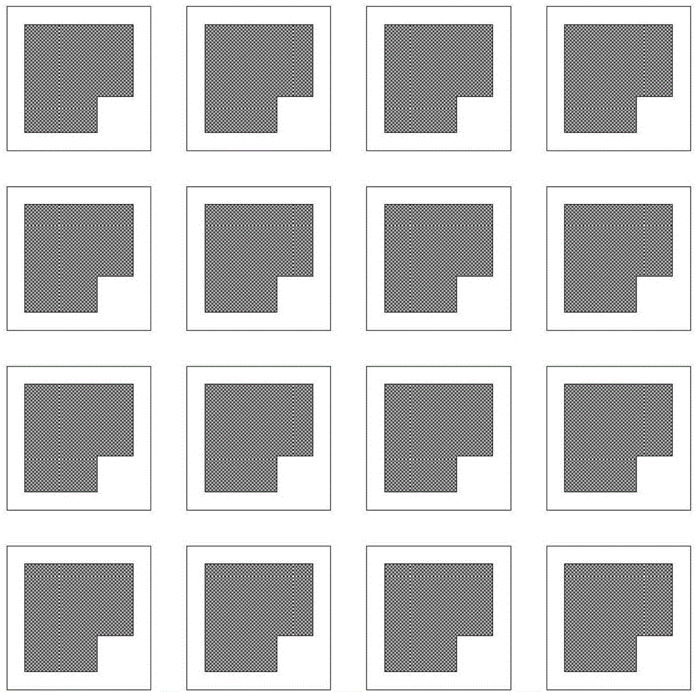
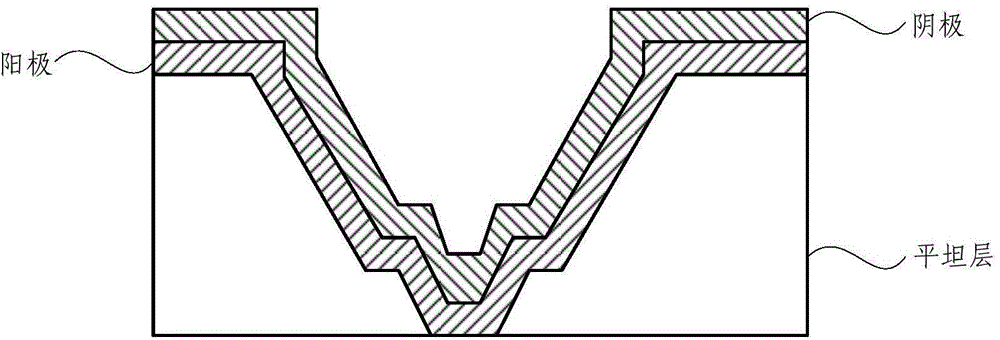
[0051] Such as Figure 7 As shown, the array substrate according to one embodiment of the present invention includes a plurality of pixel groups 13, wherein each pixel group 13 has a plurality of su...
PUM
 Abstract
Description
Claims
Application Information