Semiconductor and forming method thereof

A semiconductor and device technology, applied in the field of semiconductor manufacturing, can solve problems such as the inability to maintain the linear demand of logic circuits and the lack of carriers, and achieve the effects of shortening the production cycle, improving reliability, and improving production efficiency

Inactive Publication Date: 2015-06-03
SEMICON MFG INT (SHANGHAI) CORP
View PDF4 Cites 12 Cited by
  • Summary
  • Abstract
  • Description
  • Claims
  • Application Information

AI Technical Summary

Problems solved by technology

[0003] At present, the technology of manufacturing capacitors can be divided into two types: using polysilicon as the electrode and using metal as the electrode. Using polysilicon as the electrode will cause a lack of carriers, so that when the surface voltage across the capacitor changes, the capacitance

Method used


Image

  • Semiconductor and forming method thereof
  • Semiconductor and forming method thereof
  • Semiconductor and forming method thereof

Examples


Embodiment Construction

[0035] It can be seen from the background art that in order to meet the development of semiconductor chips toward high integration, it is more and more important to increase the capacitance per unit chip area.

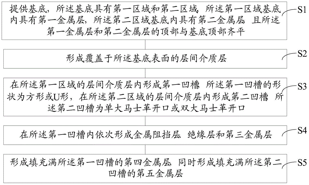
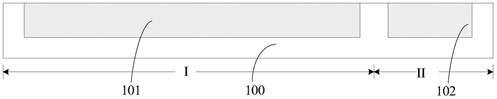
[0036] In order to solve the above problems, the formation method of semiconductor devices is studied. At present, the most common method is to form MIM capacitors while performing dual damascene process (dual damascene). Specifically, the formation method of semiconductor devices includes the following steps, please refer to figure 1 : Step S1, providing a substrate, the substrate has a first region and a second region, the first region has a first metal layer in the substrate, the second region has a second metal layer in the substrate, and the first The tops of the metal layer and the second metal layer are flush with the top of the substrate; step S2, forming an interlayer dielectric layer covering the surface of the substrate; step S3, forming a first recess in the...


PUM


Abstract

The invention provides a semiconductor and a forming method thereof, wherein the forming method of the semiconductor device comprises the following steps that a semiconductor substrate is provided, and a first interlayer dielectric layer is formed on the surface of the semiconductor substrate; a second interlayer dielectric layer is formed on the surface of the first interlayer dielectric layer; meanwhile, second interlayer dielectric layers in a first region and a second region are etched, a first groove is formed in the second interlayer dielectric layer formed in the first region, a second groove is formed in the second interlayer dielectric layer formed in the second region, in addition, the first groove comprises a first trench and a plurality of first through holes positioned at the bottom of the first trench, and a bulge is formed between the adjacent through holes; a metal blocking layer, an insulation layer and a third metal layer are sequentially formed in the first region, the metal blocking layer covers the bottom and the side wall of the first groove, and the metal blocking layer also covers the side wall and the top of the bulges. The semiconductor method and the forming method have the advantages that the mutual connection structure is formed, meanwhile, an MIM capacitor is formed, the unit area capacitance is increased, and the chip area is saved.

Description

technical field [0001] The invention relates to the field of semiconductor manufacturing, in particular to a semiconductor device and a forming method thereof. Background technique [0002] In VLSI, capacitors are one of the commonly used passive components, which are usually integrated into active components such as bipolar transistors or complementary metal oxide semiconductor (CMOS: Complementary Metal Oxide Semiconductor) transistors. [0003] At present, the technology of manufacturing capacitors can be divided into two types: using polysilicon as the electrode and using metal as the electrode. Using polysilicon as the electrode will cause a lack of carriers, so that when the surface voltage across the capacitor changes, the capacitance will also change. Therefore, capacitors with polysilicon electrodes cannot maintain the linearity requirements of today's logic circuits; capacitors with metal electrodes do not have the above problems. Such capacitors are generally call...

Claims


Application Information

Patent Timeline
IPC IPC(8): H01L21/02H01L23/522
CPCH01L21/62H01L23/5226H01L28/60
Inventor 卜伟海康劲
Owner SEMICON MFG INT (SHANGHAI) CORP
Why Eureka
Try Eureka