Array substrate, thin-film transistor and manufacturing methods thereof as well as display device

A technology of an array substrate and a manufacturing method, which are applied in the fields of display devices, array substrates, thin film transistors and manufacturing methods, can solve the problems of few manufacturing processes, high production efficiency, complicated manufacturing processes, etc., so as to reduce production costs, improve manufacturing efficiency, Reduce the effect of masking process

Active Publication Date: 2015-06-03
BOE TECH GRP CO LTD
View PDF13 Cites 30 Cited by
  • Summary
  • Abstract
  • Description
  • Claims
  • Application Information

AI Technical Summary

Problems solved by technology

[0005] Embodiments of the present invention provide an array substrate, a thin film transistor, a manufacturing method, and a display device, which are used to solve technical problems in the prior art such as complex manufacturing processes, low production efficiency, and high cost of thin film transistors and array substrates. The array substrate The structure is simple, the manufacturing process is less, so the production efficiency is high and the cost is low

Method used


Image

  • Array substrate, thin-film transistor and manufacturing methods thereof as well as display device
  • Array substrate, thin-film transistor and manufacturing methods thereof as well as display device
  • Array substrate, thin-film transistor and manufacturing methods thereof as well as display device

Examples


Embodiment Construction

[0072] The following will clearly and completely describe the technical solutions in the embodiments of the present invention with reference to the accompanying drawings in the embodiments of the present invention. Obviously, the described embodiments are only some of the embodiments of the present invention, not all of them. Based on the embodiments of the present invention, all other embodiments obtained by persons of ordinary skill in the art without creative efforts fall within the protection scope of the present invention.

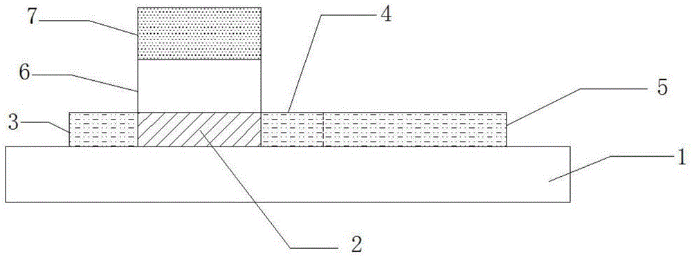
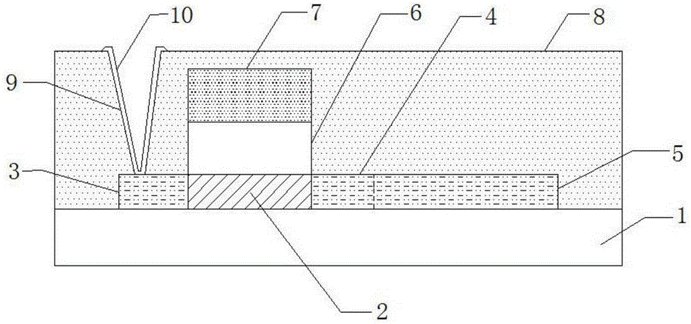
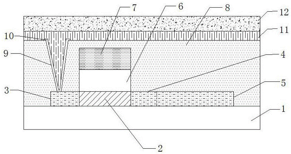
[0073] As is well known, a thin film transistor (TFT) includes: a gate, a source electrode and a drain electrode. Generally speaking, the source electrode and the drain electrode of a TFT can be regarded as equivalent; that is, among the two electrodes in the TFT except the gate, any one of them can be called the source electrode, and the other electrode can be called the drain electrode. Specifically, in the embodiments of the present invention, in o...


PUM


Abstract

The invention belongs to the technical field of display, and particularly relates to an array substrate, a thin-film transistor and manufacturing methods thereof as well as a display device. The array substrate comprises a substrate (1), and an active layer (2), a source electrode (3), a drain electrode (4) and a pixel electrode (5) which are arranged on the same layer of the substrate (1), as well as a grid insulation layer (6) positioned on the active layer (2) and a grid electrode (7) positioned on the grid insulation layer (6), wherein the active layer (2), the source electrode (3), the drain electrode (4), the pixel electrode (5), the grid insulation layer (6) and the grid electrode (7) are formed through a one-time patterning process; the source electrode (3) is connected with the drain electrode (4) through the active layer (2). The array substrate solves the technical problems that the existing array substrate is relatively complicated in structure, more in manufacturing process, low in production efficiency, relatively high in cost and the like, can substitute the existing array substrate, and is applicable to the technical field of display.

Description

technical field [0001] The invention belongs to the field of display technology, and in particular relates to an array substrate, a thin film transistor, a manufacturing method, and a display device. Background technique [0002] With the rapid development of display technology, people have higher and higher requirements for display resolution, response time, power consumption and other characteristics. In this case, with the increasing size of displays and the development of display technologies such as 3D, the mobility requirements of TFTs (Thin Film Transistor, thin film transistors) disposed on the display array substrate are getting higher and higher. The mobility of the TFT refers to the average drift velocity of carriers (electrons and holes) in the active layer of the TFT under the action of a unit electric field. In fact, using amorphous silicon to make the active layer can no longer meet the requirements for mobility, and people have begun to use metal oxide mater...

Claims


Application Information

Patent Timeline
Patent Type & Authority Applications(China)
IPC IPC(8): H01L29/786H01L29/06H01L21/28H01L27/02H01L21/77
Inventor 王珂
Owner BOE TECH GRP CO LTD
Why Eureka
Try Eureka