Wiring board and method for mounting semiconductor element on wiring board

A technology of a wiring substrate and a mounting method, which is applied in the direction of semiconductor devices, semiconductor/solid-state device components, and electrical components to assemble printed circuits, can solve problems such as the S' mounting of semiconductor components, and achieve the effect of high connection reliability.

Inactive Publication Date: 2015-06-03
KYOCERA CORP
View PDF1 Cites 2 Cited by
  • Summary
  • Abstract
  • Description
  • Claims
  • Application Information

AI Technical Summary

Problems solved by technology

Therefore, when the wiring board C thermally expands during the reflow process, a part of the solder bump H' is caught by the semiconductor element connection pad 22 and deviates, making it difficult to accurately mount the semiconductor element S' on the wiring board. The situation on C

Method used


Image

  • Wiring board and method for mounting semiconductor element on wiring board
  • Wiring board and method for mounting semiconductor element on wiring board
  • Wiring board and method for mounting semiconductor element on wiring board

Examples


Embodiment Construction

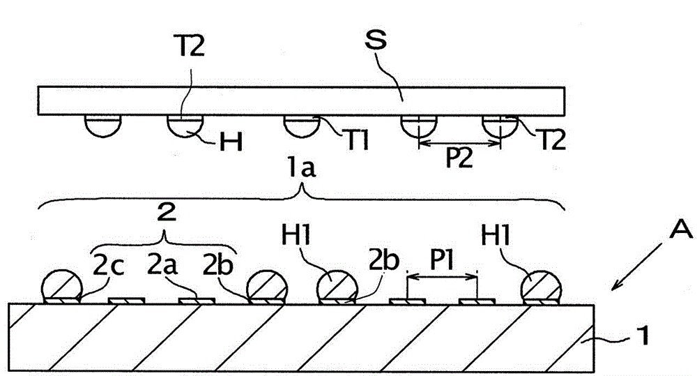
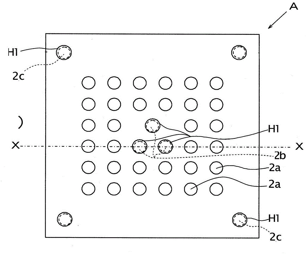
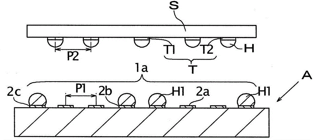
[0023] Next, based on Figure 1A as well as Figure 1B One embodiment of the wiring board of the present invention will be described. in addition, Figure 1A yes Figure 1B The X-X line profile shown. Such as Figure 1A As shown, the wiring board A of the present invention mainly includes an insulating substrate 1 and pads 2 .

[0024] The insulating substrate 1 is formed of, for example, an electrically insulating material obtained by impregnating a glass cloth with a thermosetting resin such as epoxy resin or bismaleimide triazine resin. The insulating substrate 1 has a mounting portion 1a on which a semiconductor element S is mounted on its upper surface. Figure 1A The illustrated insulating substrate 1 has a single-layer structure, but may also have a multi-layer structure in which a plurality of insulating layers made of the same or different electrically insulating materials are laminated. The semiconductor element S has a first electrode terminal T1 at the center of...


PUM


Abstract

A wiring board of the present invention includes an insulating board having a mounting portion on an upper surface to mount a semiconductor element, and semiconductor element connection pads formed on the mounting portion, on which at least three first dummy pads arranged on a center portion of the mounting portion, and at least three second dummy pads arranged on a peripheral portion of the mounting portion, are formed, and a dummy solder bump is formed on each of the first dummy pad and the second dummy pad.

Description

technical field [0001] The present invention relates to a high-density wiring board and a method of mounting semiconductor elements on the wiring board. Background technique [0002] In the prior art, when mounting a semiconductor element such as a semiconductor integrated circuit element on a wiring board, for example, as shown in FIG. 3A, a semiconductor element S' and a wiring board B are prepared. The semiconductor element S' is mainly formed of, for example, silicon, and on its lower surface, a plurality of electrode terminals T' for connecting to the wiring board B are arranged at an arrangement pitch P2', for example, in a grid pattern. A solder bump H' is attached to the electrode terminal T'. For example, JP-A-2009-188260 describes a semiconductor device in which a semiconductor chip is connected to electrodes of a mounting substrate via bumps. [0003] The wiring board B is mainly formed of a resin material such as epoxy resin, and has a mounting portion 11a on w...

Claims


Application Information

Patent Timeline
Patent Type & Authority Applications(China)
IPC IPC(8): H05K1/18H05K3/34
CPCH05K3/3436H05K2201/09781H05K2201/10674H05K2203/167H01L2224/17517H01L2224/16106H01L2224/16059H01L23/49811H01L24/16H01L24/17H01L2224/17051H01L2224/8114H01L2224/81194H01L2224/81447H01L2224/81815H01L2224/16108H01L23/49816H01L23/49838H01L2224/131H01L24/81H01L2224/81193H01L2924/351H01L2924/381Y02P70/50H01L2924/00014H01L2924/014
Inventor 祢占孝之
Owner KYOCERA CORP
Why Eureka
Try Eureka