
Alignment mark structure for photoetching and manufacturing method thereof

A technology for lithography alignment and alignment marks, which is applied in microlithography exposure equipment, optics, and photographic plate-making processes on patterned surfaces, etc., and can solve layout design and publication limitations, poor alignment, and vector fitting Questioning and other issues to achieve the effect of solving the lack of cutting space, reducing errors and high-order parts, and avoiding unpredictability

Active Publication Date: 2015-06-10
SHANGHAI HUALI MICROELECTRONICS CORP
View PDF5 Cites 17 Cited by
  • Summary
  • Abstract
  • Description
  • Claims
  • Application Information

AI Technical Summary

Problems solved by technology

[0005] 1. The placement of traditional alignment measurement patterns occupies more layout design space. On 2-in-1, 4-in-1, and N-in-1 masks, the space for cutting lines will become smaller and smaller, but the required test patterns However, it cannot be reduced. The space occupied by traditional alignment patterns will force the reticle to discard some test patterns before publication, and small layout design and publication will also be limited by this;
[0006] 2. The traditional alignment measurement graphics cannot measure the alignment accuracy across layers without increasing the number of additional front-layer alignment graphics, for example, when the second layer has a deviation from the first layer alignment , then it is no longer possible to use the third level to directly calibrate the method of the first level, but can only continue to align with the second level that already has deviations;
[0007] 3. When the traditional alignment measurement pattern is applied to the double exposure double patterning of the advanced process, it is difficult to improve the alignment error and residual problems. The reason is that it is limited by the single-level alignment of the traditional alignment measurement pattern. When performing the second In the exposure type, different front-layer marks need to be selected for alignment measurement, and it is obviously impossible to fix the same front-layer mark for measurement;
[0008] 4. When the traditional alignment measurement pattern adds a new pattern layer, it is necessary to add an additional front-layer alignment mark. In this way, it is necessary to re-publish the 2-layer mask including the front-layer mask, which increases additional costs;
Although this structure can perform three-layer alignment at the same time, the design cannot cover the deviation collection in the X and Y directions at the same time, and the vector fitting degree is questionable. This is also true for the development of chip structures below 28 nanometers. There is a risk of misalignment
And the current lithography technology no longer stays in the way of 2 exposures (double exposure), but has risen to 3 exposures, or even 4 exposures. This structure also cannot be used for subsequent multi-layer mark alignment through fixed front-layer marks. Measure

Method used


Image

  • Alignment mark structure for photoetching and manufacturing method thereof
  • Alignment mark structure for photoetching and manufacturing method thereof
  • Alignment mark structure for photoetching and manufacturing method thereof

Examples


Embodiment Construction

[0048] In order to make the purpose and features of the present invention more obvious and easy to understand, the following will further describe the specific embodiments of the present invention in conjunction with the accompanying drawings. However, the present invention can be realized in different forms, and should not be considered as being limited to the described embodiments . It should be noted that the relative arrangements of components and steps, numerical expressions and numerical values ​​set forth in these embodiments do not limit the scope of the present invention unless specifically stated otherwise. At the same time, it should be understood that, for the convenience of description, the sizes of the various parts shown in the drawings are not drawn according to the actual proportional relationship. The following description of at least one exemplary embodiment is merely illustrative in nature and in no way taken as limiting the invention, its application or us...


PUM


Abstract

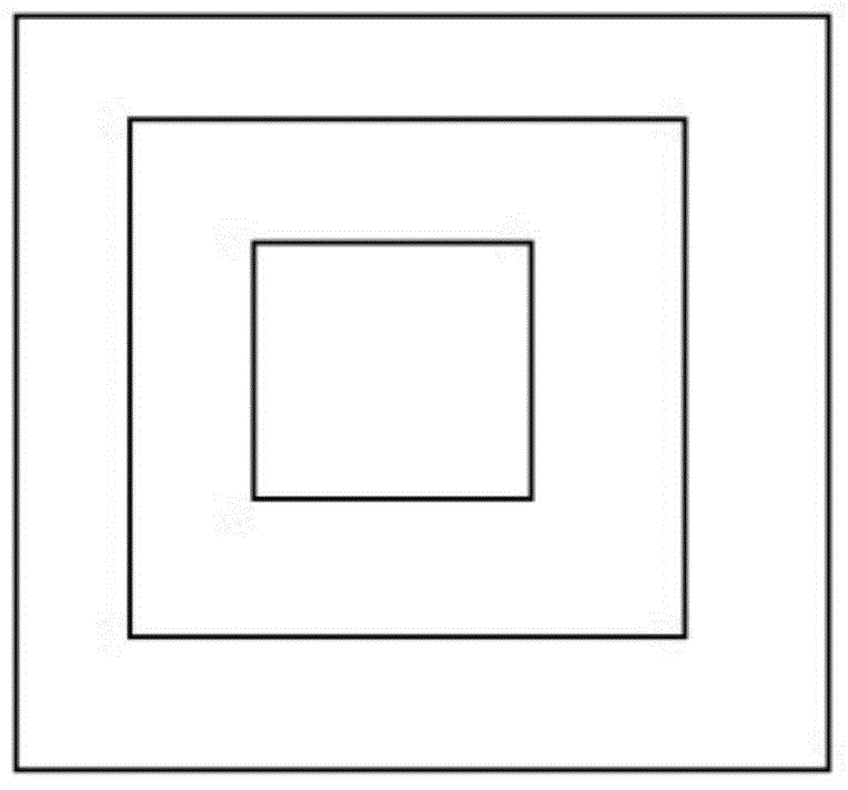
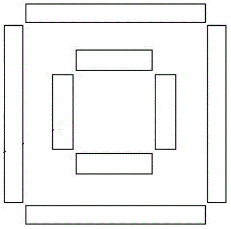
The invention provides an alignment mark structure for photoetching and a manufacturing method thereof and relates to the design and manufacturing method of a multi-layer graph structure for mutual alignment precision. According to the alignment mark structure for photoetching and a manufacturing method of the alignment mark structure, all photoetching alignment graphs are centrally symmetrical about the same center when the photoetching alignment graphs are projected to the plane where any of the photoetching alignment graphs is located, the projections of all the photoetching alignment graphs are nested and expand in sequence from inside to outside in the forming sequence of the photoetching alignment graphs, the alignment mark structure can be applied to the manufacturing processes based on various photoetching techniques, free matching can be conducted according to different requirements, the requirement for alignment of various photoetching techniques can be met, the requirement for alignment of photoetching alignment marks on different layers can be met, the requirements for traditional alignment measurement and alignment measurement required by three-time exposure and four-time exposure can also be met, the space of a cutting way can be saved, and cost is reduced.

Description

technical field [0001] The invention relates to the field of semiconductor manufacturing, in particular to a photolithographic alignment mark structure and a manufacturing method thereof. Background technique [0002] With the continuous improvement of integrated circuit manufacturing technology and the continuous shrinking of line width, the area of ​​semiconductor devices is becoming smaller and smaller, and the layout of semiconductors has evolved from ordinary single-function separation devices to integrated high-density and multi-functional integrated circuits; From the initial IC (integrated circuit) to LSI (large-scale integrated circuit), VLSI (very large-scale integrated circuit), until today's ULSI (ultra-large-scale integrated circuit), the area of ​​the device is further reduced, and the functions are more comprehensive and powerful. Considering the complexity of process research and development, long-term and high cost and other unfavorable factors, how to furth...

Claims


Application Information

Patent Timeline
Patent Type & Authority Applications(China)
IPC IPC(8): G03F7/20G03F9/00
Inventor 王艳云毛智彪杨正凯罗华明
Owner SHANGHAI HUALI MICROELECTRONICS CORP
Learn More