

Display panel and manufacturing method thereof as well as display device
一种显示面板、制造方法的技术,应用在显示装置,显示面板及其制造领域,能够解决边框区颜色偏暗、遮蔽层厚度大、影响美观等问题,达到降低厚度的效果
- Summary
- Abstract
- Description
- Claims
- Application Information
AI Technical Summary
Problems solved by technology
Method used
Image

Examples
Embodiment 1
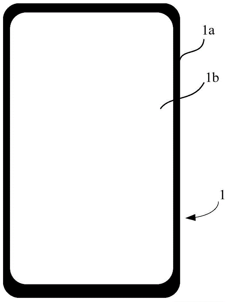
[0045] An embodiment of the present invention provides a display panel, see figure 1 , the display panel includes a transparent substrate 1, the transparent substrate 1 is divided into a frame area 1a and a display area 1b, and the frame area 1a is arranged around the display area 1b.
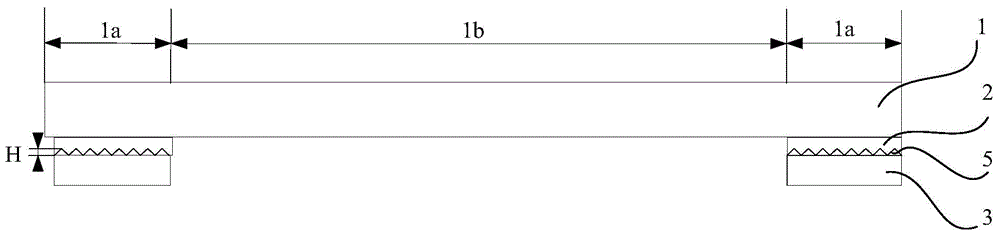
[0046] combine figure 2 , figure 2 for figure 1 A schematic cross-sectional view of the display panel shown, as figure 2 As shown, the display panel also includes a non-black photoresist layer 2 and a black photoresist layer 3, the non-black photoresist layer 2 and the black photoresist layer 3 are sequentially arranged on the frame area 1a of the transparent substrate 1, and the black photoresist layer 2 and the non-black photoresist layer 3 are provided with a diffuse reflection structure 5 .
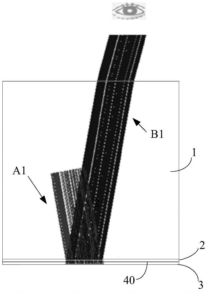
[0047] Figure 3a and Figure 3b The shielding layer of the display panel in the embodiment of the present invention and the shielding layer of the existing display panel reflect the light inc...
Embodiment 2
[0057] An embodiment of the present invention provides a display panel. In this embodiment, the display panel is an OGS (One Glass Solution, integrated touch) panel. see Figure 4 , the display panel includes a transparent substrate 1, the transparent substrate 1 is divided into a frame area 1a and a display area 1b, and the frame area 1a is arranged around the display area 1b.
[0058] combine Figure 5 , Figure 5 for Figure 4 The schematic cross-sectional view of the display panel along the X direction, such as Figure 5 As shown, the display panel also includes a non-black photoresist layer 2, a black photoresist layer 3 and an electrode layer 4. The non-black photoresist layer 2 and the black photoresist layer 3 are sequentially arranged on the frame area 1a of the transparent substrate 1, and the black photoresist layer The junction surface of the photoresist layer 2 and the non-black photoresist layer 3 is provided with a diffuse reflection structure 5 . The elect...
Embodiment 3
[0074] The structure of the display panel provided in this embodiment is basically the same as the structure of the display panel in Embodiment 2, the difference is that, as Image 6 As shown, the display panel of this embodiment may further include an FPC (Flexible Printed Circuit board, flexible printed circuit board) 7 with a touch IC (Integrated Circuit, integrated circuit) chip, and the FPC 7 is electrically connected to the electrode layer 4 .
[0075] It should be noted that, for simplicity, Image 6 The specific structure of the electrode layer 4 is not shown in the figure.
[0076] Since the structure of the display panel in this embodiment is basically the same as the structure of the display panel in the second embodiment, it has the same effect as the display panel provided in the second embodiment.
[0077] In addition, the display panel of this embodiment may further include a protective layer 6 formed on the electrode layer 4 . The protection layer 6 can be an...
PUM
 Abstract
Description
Claims
Application Information