A method of forming a semiconductor device

A semiconductor and device technology, applied in the field of semiconductor preparation, can solve the problems affecting the process of metal deposition process, affecting the quality of gate, difficult to remove by-products, etc., to achieve the effect of inhibiting the formation of by-products and avoiding ion diffusion

Active Publication Date: 2017-11-03
SEMICON MFG INT (SHANGHAI) CORP
View PDF4 Cites 0 Cited by
  • Summary
  • Abstract
  • Description
  • Claims
  • Application Information

AI Technical Summary

Problems solved by technology

[0005] However, in the actual operation process, it is found that after the etching of the hard mask layer 13 is completed, a large number of by-products will be left on the semiconductor substrate and in the photoresist layer 15, and these by-products are difficult to remove. Thus affecting the process of a series of processes such as subsequent metal deposition, and ultimately affecting the quality of the subsequently formed gate

Method used


Image

  • A method of forming a semiconductor device
  • A method of forming a semiconductor device
  • A method of forming a semiconductor device

Examples


Embodiment Construction

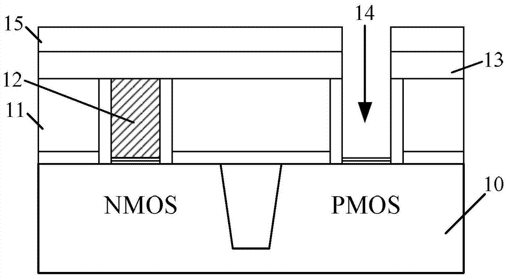
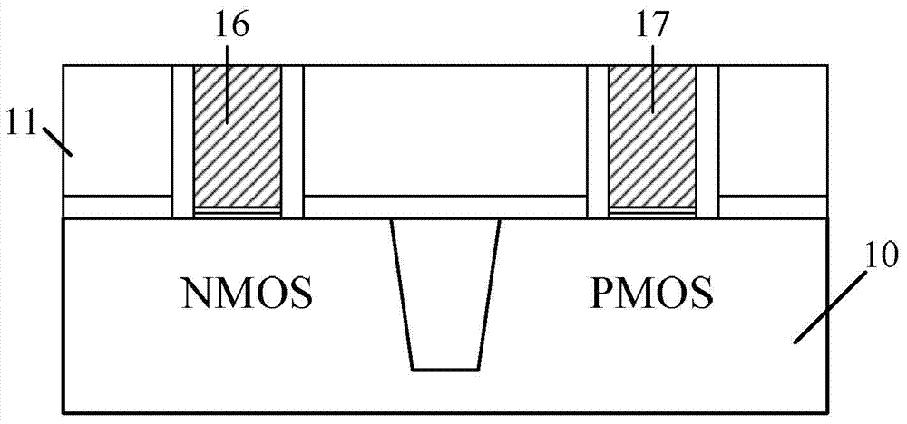
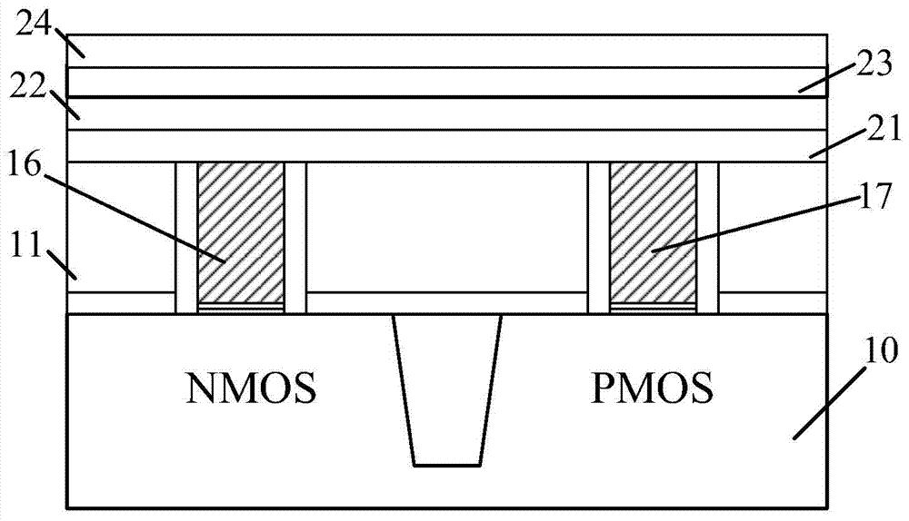
[0031] As mentioned in the background art, with the increase of the integration level of integrated circuits, the device size of integrated circuits decreases continuously, and the quality requirements for devices become more and more stringent. For example, in the CMOS gate preparation process, the last gate (gate last) process has gradually replaced the front gate (gate first) process, so as to avoid the formation of the source region and the drain region in the front gate process, after the source and drain ion implantation is completed. The annealing process causes damage to the gate.

[0032] However, in the actual operation of the gate-last process, it is found that when the patterned photoresist layer is used to etch the hard mask layer, thereby exposing the dummy gate to be etched, and using the hard mask layer as a mask to etch In the process of removing the dummy gate by etching, a large number of by-products will be formed, and these by-products are difficult to rem...


PUM


Abstract

The invention provides a formation method of a semiconductor device. The formation method includes steps of forming a hard masking layer on a semiconductor substrate, forming a barrier layer above the hard masking layer, and forming a photoresist layer on the barrier layer. Since the barrier layer is formed between the photoresist layer and the hard masking layer, ion diffusion between the hard masking layer and the photoresist layer is effectively avoided, and formation of side products is effectively prohibited. In addition, the patternized photoresist layer is the masked and etched barrier layer, and the etched barrier layer is the masked and etched hard masking layer after the photoresist layer is removed, and hard masking patterns are formed in the hard masking layer. Compared with the prior art, the formation method of the semiconductor device is capable of effectively avoiding reaction between photoresist, etching gas, fake grid materials and the hard masking layer to generate side products hard to remove to affect successive semiconductor preparation process when the hard masking layer is etched, and performance of the semiconductor device is finally formed.

Description

technical field [0001] The invention relates to the field of semiconductor preparation, in particular to a method for forming a semiconductor device. Background technique [0002] With the development of integrated circuit manufacturing technology, the integration degree of integrated circuits is increasing, and the feature size of integrated circuits is also decreasing, and the quality requirements for electrical components in integrated circuits are becoming more and more stringent. The integrated circuit manufacturing process is also constantly innovating to improve the quality of the manufactured integrated circuit electrical components. [0003] For example, in the gate preparation process of COMS, the gate last process has gradually replaced the gate first process to improve the quality of the gate. The so-called gate-front process means that after forming an opening in the dielectric layer of the semiconductor substrate, the gate material is directly filled in the op...

Claims


Application Information

Patent Timeline
Patent Type & Authority Patents(China)
IPC IPC(8): H01L21/027H01L21/28
CPCH01L21/027H01L21/28008
Inventor 隋运奇
Owner SEMICON MFG INT (SHANGHAI) CORP
Why Eureka
Try Eureka