VDMOS field effect transistor and forming method thereof

A field effect transistor, polysilicon layer technology, applied in semiconductor devices, semiconductor/solid-state device manufacturing, electrical components, etc., can solve the problems of complex epitaxial layer growth process and high cost, and achieve the promotion of technological progress, low cost, and increased application. range effect

Active Publication Date: 2015-06-10
SEMICON MFG INT (SHANGHAI) CORP
View PDF5 Cites 1 Cited by
  • Summary
  • Abstract
  • Description
  • Claims
  • Application Information

AI Technical Summary

Problems solved by technology

[0011] The problem solved by the present invention is that the epitaxial layer growth process in the existing VDMOS field effect transistor is complicated and the cost is high

Method used


Image

  • VDMOS field effect transistor and forming method thereof
  • VDMOS field effect transistor and forming method thereof
  • VDMOS field effect transistor and forming method thereof

Examples


Embodiment Construction

[0065] In order to make the above objects, features and advantages of the present invention more comprehensible, specific embodiments of the present invention will be described in detail below in conjunction with the accompanying drawings.

[0066] An embodiment of the present invention provides a method for forming a VDMOS field effect transistor.

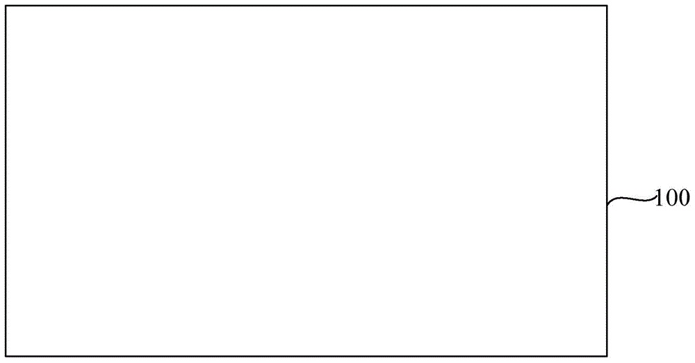
[0067] refer to figure 2 , providing a substrate 100 with a first type of doping. In this embodiment, the first type of doping can be P-type doping or N-type doping, usually P-type doping is selected.

[0068] In a specific embodiment, the substrate 100 may be a silicon substrate, a germanium substrate, or a silicon-on-insulator substrate, etc.; or the material of the substrate 100 may also include other materials, such as III-V compounds such as gallium arsenide. Those skilled in the art can select the substrate according to needs, so the type of the substrate should not limit the protection scope of the present invention.

...


PUM


Abstract

Disclosed are a VDMOS field effect transistor and a forming method thereof. The method includes providing a substrate provided with a first type dopant; forming first and second grooves in the substrate; forming a first insulation layer on the side wall of the first groove, and forming a second insulation layer on the side wall of the second groove; filling the first groove with a first polycrystalline silicon layer with the second type dopant, and filling the second groove with a second polycrystalline silicon layer with the second type dopant; forming a first buried layer with the second type dopant on the substrate below the first polycrystalline silicon layer, and forming a second buried layer with the second type dopant on the substrate below the second polycrystalline silicon layer; forming a first well region on the substrate between the first and second polycrystalline silicon layers in a doped manner; forming a second well region on the first well region; forming a first gate electrode on the first well region; forming a first source electrode on the second well region and forming a first leakage electrode on the upper surface of the first polycrystalline silicon layer. By the aid of the telescopic scheme, the extension growing process is omitted, and cost is low.

Description

technical field [0001] The invention relates to the technical field of semiconductors, in particular to a VDMOS field effect transistor and a forming method thereof. Background technique [0002] As a kind of power device, Vertical Double-diffused Metal-Oxide Semiconductor (VDMOS) field effect transistor is widely used due to its advantages of high input impedance and low conduction voltage drop. [0003] refer to figure 1 , existing VDMOS FETs include: [0004] A substrate 1 with N+ doping, the substrate 1 includes a front side S1 and a back side S2; [0005] An epitaxial layer 2 with N+ doping located on the front side S1 of the substrate 1; [0006] A gate dielectric layer 3 on the epitaxial layer 2 and a gate 4 on the gate dielectric layer 3; [0007] The P well region 5 located in the epitaxial layer 2 around the gate 4 and the source 6 located in the P well region 5, the source 6 is close to the gate 4, and the P well region 5 partially extends under the gate diele...

Claims


Application Information

Patent Timeline
IPC IPC(8): H01L21/336H01L29/78H01L29/10
Inventor 刘丽王刚宁冯喆韻唐凌
Owner SEMICON MFG INT (SHANGHAI) CORP
Why Eureka
Try Eureka