Chip packaging structure with electromagnetic shielding function

A chip packaging structure, electromagnetic shielding technology, applied in the direction of circuits, electrical components, electric solid devices, etc., can solve the problems of application limitations, miniaturization of device packaging, package cost and volume increase, and achieve the goal of saving metal materials Effect

Inactive Publication Date: 2015-06-10
JIANGYIN CHANGDIAN ADVANCED PACKAGING CO LTD
View PDF5 Cites 12 Cited by
  • Summary
  • Abstract
  • Description
  • Claims
  • Application Information

AI Technical Summary

Problems solved by technology

However, the existence of the electromagnetic shielding metal shell as an additional component often results in a multiplied increase in the cost and volume of the package. This package structure is contrary to the trend of miniaturization of device packaging and is in line with the concept of green energy advocated by modern society. Contradiction, its application will be greatly limited

Method used


Image

  • Chip packaging structure with electromagnetic shielding function
  • Chip packaging structure with electromagnetic shielding function
  • Chip packaging structure with electromagnetic shielding function

Examples


Embodiment 2

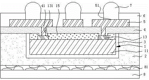
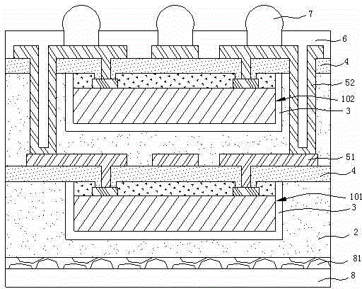
[0049] Embodiment two, see Figure 4

[0050] The packaging structure of Embodiment 2 is basically similar to that of Embodiment 1, the difference being:

[0051] In order to enhance heat dissipation and improve the reliability of the chip packaging structure, the electromagnetic shielding layer 3 made of iron, copper, nickel and their alloys with thermal conductivity can also extend outward along the upper surface of the encapsulation body 2 to expand its extension area ,Such as Figure 4 shown. The re-passivation layer 4 directly covers the front surface of the chip 1 and the upper surface of the electromagnetic shielding layer 3 .

[0052]A chip packaging structure with electromagnetic shielding function of the present invention is not limited to the above-mentioned preferred embodiments, such as the horizontal height of the electromagnetic shielding layer 3 on the side wall of the chip 1 is higher than the horizontal height of the front of the chip 1 to further ensure t...


PUM


Abstract

The invention relates to a chip packaging structure with the electromagnetic shielding function, and belongs to the technical field of semiconductor packaging. The chip packaging structure with the electromagnetic shielding function comprises a chip of the front surface is equipped with a chip electrode, and an encapsulating body; the encapsulating body comprises an encapsulating chip; electromagnetic shielding layers are arranged on the rear surface and four side surfaces of the chip; repassivation layers are arranged on the front surface of the chip and the upper surface of the encapsulating body; repassivation layer openings which expose from the upper surface of the chip electrode are formed in the repassivation layers, positioned above the chip electrode; a re-wiring metal layer and a surface protecting layer are selectively arranged on the surface of each repassivation layer, wherein the re-wiring metal layers are connected with the chip electrode through the repassivation layer openings, and the input / output ends are arranged on the upper surfaces of the re-wiring metal layers; the surface protecting layer covers the surfaces of the re-wiring metal layers, outside the input / output end. With the adoption of the chip packaging structure with the electromagnetic shielding function, the cost and size of the packaging body are unchanged, so that the development trend of small packaging of a device is met.

Description

technical field [0001] The invention relates to a chip packaging structure with electromagnetic shielding function, belonging to the technical field of semiconductor packaging. Background technique [0002] With the popularization and application of wireless connections, the number of frequency conversion radio frequency device modules used in the same module has increased sharply, resulting in electromagnetic interference between devices, between modules, and between devices. Interference is getting worse. A general method for shielding electromagnetic interference is to add an appropriate electromagnetic shielding metal shell made of metal outside the package body, and the thicker the electromagnetic shielding metal shell, the better the shielding effect on electromagnetic waves. However, the existence of the electromagnetic shielding metal shell as an additional component often results in a multiplied increase in the cost and volume of the package. This package structure...

Claims


Application Information

Patent Timeline
Patent Type & Authority Applications(China)
IPC IPC(8): H01L23/31H01L23/552H01L23/367H01L23/373
CPCH01L2224/04105H01L2224/12105H01L2224/18H01L2224/32225H01L2224/32245H01L2224/73267H01L2924/15153H01L2924/3025
Inventor 张黎赖志明陈栋陈锦辉
Owner JIANGYIN CHANGDIAN ADVANCED PACKAGING CO LTD
Why Eureka
Try Eureka