PCB (printed circuit board) heat-radiation soldering pad used for QFN (quad flat no-lead package) chip, and QFN chip and PCB soldering method

A technology of heat dissipation pad and welding method, which is applied in the directions of printed circuit parts, electrical components, electric solid devices, etc., can solve the problems of reduced solder volume, poor soldering, and inability to reach the soldering surface.

Active Publication Date: 2015-06-10
SHENZHEN GONGJIN ELECTRONICS CO LTD
View PDF5 Cites 17 Cited by
  • Summary
  • Abstract
  • Description
  • Claims
  • Application Information

AI Technical Summary

Problems solved by technology

However, when mounting QFN devices, in order to ensure the quality of soldering, the via holes opened on the heat dissipation pad are usually blocked with ink on the side that does not need to be soldered (that is, the back of the PCB). The purpose is to prevent the heat dissipation pad from When the solder on the heat sink passes through the furnace, the solder on the heat dissipation pad will flow to the non-soldering surface through the via hole, resulting in a decrease in the amount of solder on the soldering surface. If the amount of solder is reduced, it will lead to poor soldering; If it is blocked, it will not be able to play the role of the original auxiliary gas escape

Method used


Image

  • PCB (printed circuit board) heat-radiation soldering pad used for QFN (quad flat no-lead package) chip, and QFN chip and PCB soldering method
  • PCB (printed circuit board) heat-radiation soldering pad used for QFN (quad flat no-lead package) chip, and QFN chip and PCB soldering method
  • PCB (printed circuit board) heat-radiation soldering pad used for QFN (quad flat no-lead package) chip, and QFN chip and PCB soldering method

Examples


Embodiment Construction

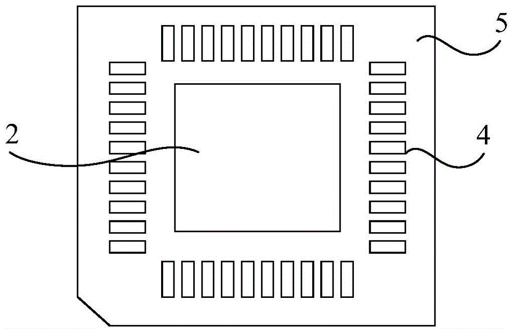
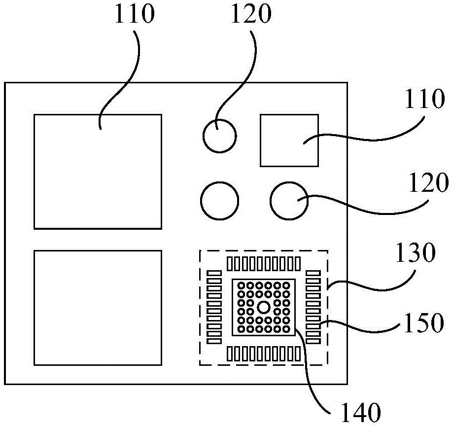
[0026] Such as image 3 Shown is a schematic diagram of the PCB planar structure of an embodiment. QFN chips can be mounted on the PCB 10 . Various chips 110 and components 120 can be mounted on the PCB 10 , and the chips 110 and components 120 are interconnected through wires embedded in the PCB 10 . In order to mount the QFN chip, the PCB 10 is provided with a pad area 130 for soldering the QFN chip. The pad area 130 has a thermal pad 140 and a lead pad 150 surrounding the thermal pad 140 . The heat dissipation pad 140 is consistent with the size of the exposed pad of the QFN chip to be soldered, and the number and size of the pin pads 150 are consistent with the number and size of the pin area of ​​the QFN chip to be soldered.

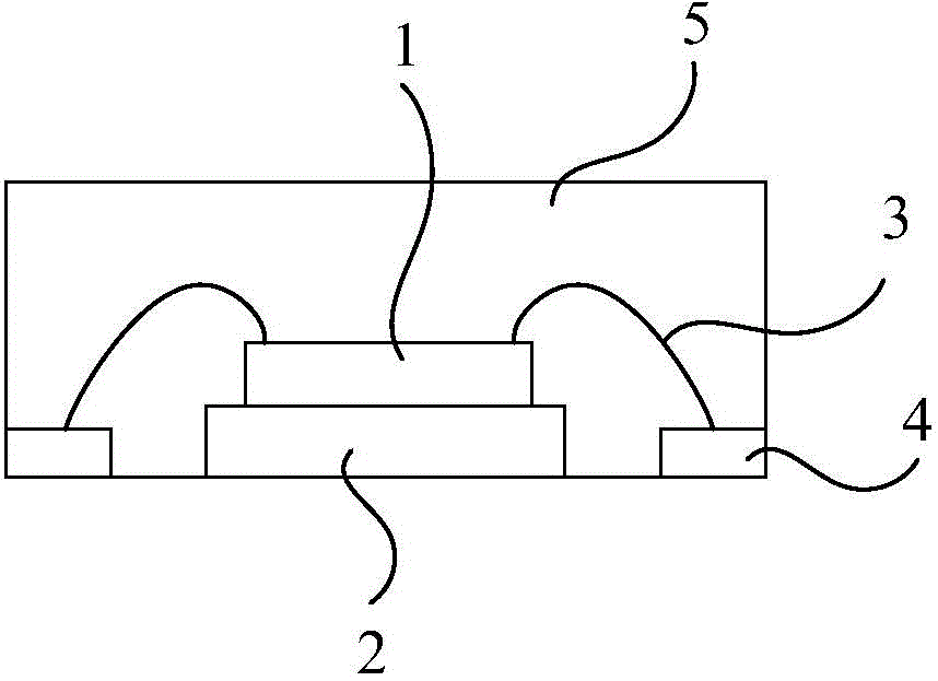
[0027] Such as Figure 4 Shown is an enlarged view of the thermal pad 140 . The heat dissipation pad 140 is a metal plate with good thermal conductivity, such as an aluminum plate or a copper plate. The metal plate body is provided with a heat...


PUM


Abstract

The invention discloses a PCB (printed circuit board) heat-radiation soldering pad used for a QFN (quad flat no-lead package) chip. The PCB heat-radiation soldering pad is provided with heat radiation via holes not larger than 0.3 mm in diameter and escape holes 0.8-1.2 mm in diameter. The invention further discloses a soldering method adopting the heat-radiation soldering pad. The soldering method includes printing ink used for plugging the heat radiation via holes on one side of a PCB which does not need soldering in correspondence to the heat-radiation soldering pad; painting tin paste on the heat-radiation soldering pad by a mesh plate without holes corresponding to the escape holes; attaching the QFN chip to the corresponding position of the PCB, so as to enable the QFN chip to expose to be flush with the PCB heat-radiation soldering pad and a pin area of the QFN chip with a PCB pin soldering pad; soldering the QFN chip on the PCB by reflow soldering. By the method, gas escape can be helped in the soldering process via the escape holes, soldering tin outflow can be prevented and good soldering effect is achieved.

Description

technical field [0001] The invention relates to printed circuit board welding, in particular to a PCB heat dissipation pad used for QFN packaged chips and a method for welding QFN chips and PCBs. Background technique [0002] QFN (Quad Flat No-lead Package) is a high power density package. figure 1 is a schematic cross-sectional view of the QFN package structure, figure 2 is the bottom view of the QFN chip. refer to figure 1 and figure 2 , Chip 1 is placed on exposed pad (exposed pad) 2 . The functional terminal on the chip 1 is electrically connected to the lead area 4 arranged around the exposed pad 2 through the wire 3 . Finally, the chip 1 is wrapped and packaged by the package body 5 . Wherein the exposed pad 2 and the lead area 4 are both exposed on one side of the package body 5 . [0003] When the QFN chip is mounted on the PCB, it is welded on the PCB in a bonded form. The pin area 4 of the QFN chip corresponds to the pad at the corresponding position on t...

Claims


Application Information

Patent Timeline
Patent Type & Authority Applications(China)
IPC IPC(8): H01L23/498H01L21/60H05K1/02
CPCH01L2224/48091H01L2224/48247H01L2924/00014
Inventor 王达国
Owner SHENZHEN GONGJIN ELECTRONICS CO LTD
Why Eureka
Try Eureka