Thin film transistor array substrate and preparation method thereof, display device
A technology for thin film transistors and array substrates, applied in the display field, can solve the problems of gate transfer electrostatic discharge, gate easily corroded, and high production cost of mask plates, so as to reduce the risk of gate corrosion and reduce production costs. Effect
- Summary
- Abstract
- Description
- Claims
- Application Information
AI Technical Summary
Problems solved by technology
Method used
Image

Examples
Embodiment 1
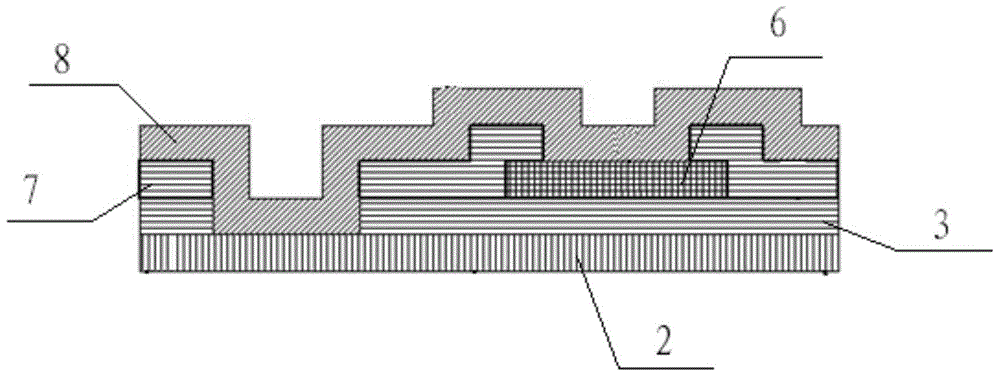
[0052] Such as Figure 5As shown, this embodiment provides a thin film transistor array substrate, including: a display area and a frame area surrounding the display area, wherein the display area includes:
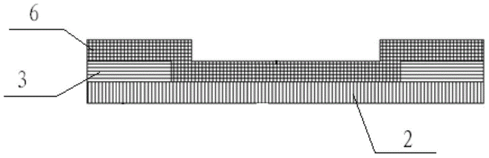
[0053] The substrate 1 and the gate electrode 2, the first insulating layer 3, the active layer 4, the etch stop layer 5, the source and drain electrodes 6, the second insulating layer 7 and the pixel electrode 8 formed sequentially on the substrate 1, in the The pattern of the second insulating layer 7 in the display area is the same as that of the etching stopper layer 5 .
[0054] In this embodiment, the same mask is used to prepare the second insulating layer 7 and the etching stopper layer 5, which saves a mask and reduces production costs; at the same time, the second insulating layer in the display area The pattern of the layer 7 is the same as that of the etching barrier layer 5, which ensures that the pixel electrode 8 is connected to the drain through the via h...
Embodiment 2
[0061] This embodiment provides a method for preparing the above-mentioned thin film transistor array substrate, which includes forming various functional layers in the display area of the thin film transistor array substrate and the frame area surrounding the display area by adopting the following steps: specifically,
[0062] Such as Figure 8 As shown, a gate 2 is formed on a substrate 1 through a patterning process, and a gate mask can be used in this step;
[0063] Such as Figure 9 As shown, the first insulating layer 3 (gate insulating layer) is deposited on the substrate 1 forming the gate 2; the first insulating layer mask is used in this step (referred to as 6-mask process at this time), also If this step is not used, it is called a 5-mask process.
[0064] Such as Figure 10 As shown, the active layer 4 is formed on the substrate 1 on which the first insulating layer 3 is deposited by a patterning process, and an active layer mask is used in this step;
[0065...
Embodiment 3
[0080] This embodiment provides a display device, which includes the above thin film transistor array substrate.
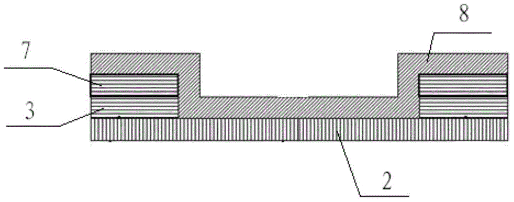
[0081] The thin-film transistor array substrate and the preparation method thereof of the present invention, and the display device use the same mask plate when preparing the second insulating layer 7 and the etching stopper layer 5, which saves a mask plate and reduces the production cost; at the same time , in the display area, the pattern of the second insulating layer 7 is the same as that of the etching stopper layer 5, which ensures that the pixel electrode 8 is connected to the drain through the via hole; in the frame area, the source and drain electrodes 6 directly cover the When the gate 2 and the source and drain 6 are made of corrosion-resistant metals, the risk of corrosion of the gate 2 and the risk of electrostatic discharge of the transfer of the gate 2 can be reduced.
PUM
 Abstract
Description
Claims
Application Information
 - R&D
- Intellectual Property
- Life Sciences
- Materials
- Tech Scout
- Unparalleled Data Quality
- Higher Quality Content
- 60% Fewer Hallucinations
Browse by: Latest US Patents, China's latest patents, Technical Efficacy Thesaurus, Application Domain, Technology Topic, Popular Technical Reports.
© 2025 PatSnap. All rights reserved.Legal|Privacy policy|Modern Slavery Act Transparency Statement|Sitemap|About US| Contact US: help@patsnap.com