Thin film transistor, preparation method thereof, array substrate and display device

A thin-film transistor and thin-film technology, applied in the direction of transistors, semiconductor/solid-state device manufacturing, electric solid-state devices, etc., can solve the problems of strong diffusion ability of electrodes or wires, poor display devices, and easy oxidation, so as to improve anti-oxidation ability and avoid Bad display device, avoid the effect of bad display device or abnormal display

Inactive Publication Date: 2015-06-10
BOE TECH GRP CO LTD
View PDF3 Cites 18 Cited by
  • Summary
  • Abstract
  • Description
  • Claims
  • Application Information

AI Technical Summary

Problems solved by technology

[0004] The object of the present invention is to provide a thin film transistor and its preparation method, an array substrate and a display device, to solve the problem that the display device is defective or displays abnormally due to the strong diffusion ability or easy oxidation of electrodes or wires made of Cu

Method used


Image

  • Thin film transistor, preparation method thereof, array substrate and display device
  • Thin film transistor, preparation method thereof, array substrate and display device
  • Thin film transistor, preparation method thereof, array substrate and display device

Examples


Embodiment 1

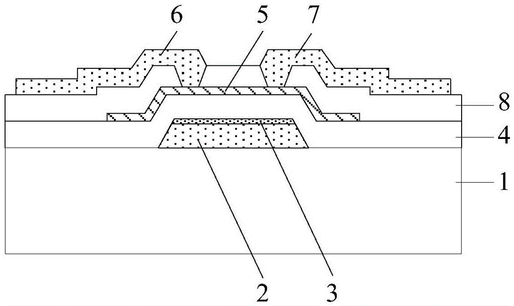
[0034] see figure 1 The first thin film transistor provided by the embodiment of the present invention includes a base substrate 1, a gate electrode 2 formed of pure copper material, a gate insulating layer 4, an active layer 5, a source electrode 6, and a drain electrode 7. The thin film transistor also The copper alloy film layer 3 is included, and the copper alloy film layer 3 is arranged on the side of the gate electrode 2 facing the active layer 5 . In this embodiment, a copper alloy film layer 3 is provided on the side of the gate electrode 2 of the thin film transistor facing the active layer 5, and the accumulation of alloy elements in the copper alloy film layer 3 at grain boundaries, crystal planes, and surfaces can prevent copper atoms from Diffusion to the active layer 5 can also improve the oxidation resistance of the gate electrode 2, thereby avoiding the failure of the thin film transistor or the problem of poor display or abnormal display caused by mura defects...

Embodiment 2

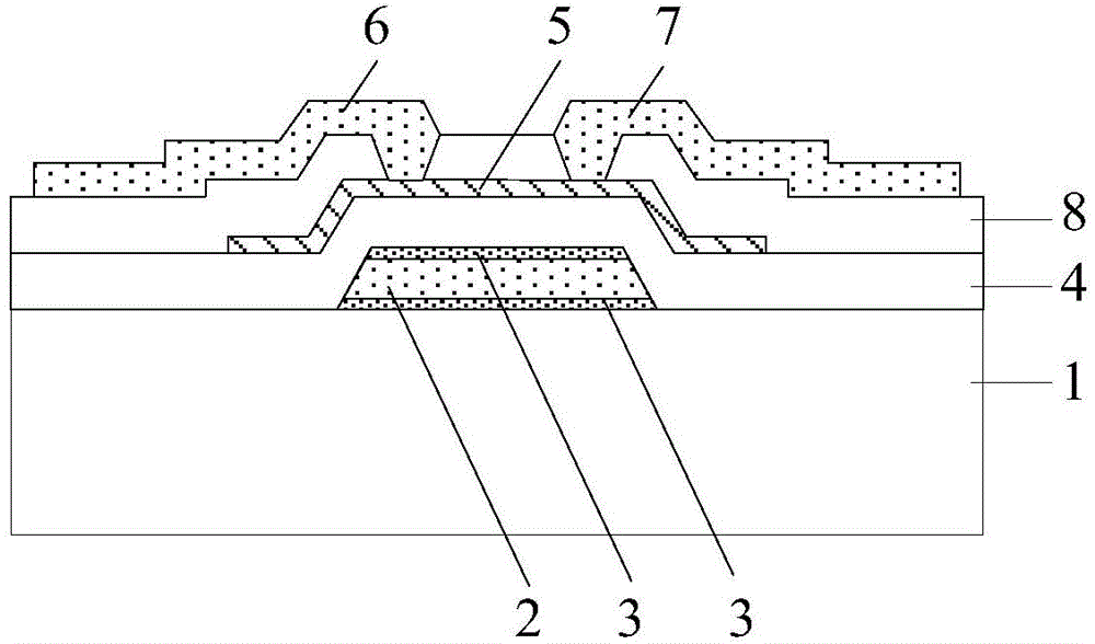
[0039] see figure 2 The second thin film transistor provided by the embodiment of the present invention includes a base substrate 1, a gate electrode 2 formed of pure copper material, a gate insulating layer 4, an active layer 5, a source electrode 6, and a drain electrode 7. The thin film transistor also The copper alloy film layer 3 is included, and the copper alloy film layer 3 is arranged on the side of the gate electrode 2 facing the active layer 5 . and figure 1 The TFT shown is different in that a copper alloy film layer 3 is also provided on the side of the gate electrode 2 of the TFT that faces away from the active layer 5 . In this embodiment, a copper alloy film layer 3 is provided above and below the gate electrode 2 of the thin film transistor, and the alloy elements in the copper alloy film layer 3 accumulate at grain boundaries, crystal planes, and surfaces, for example, the gate electrode 2 faces the The accumulation of alloy elements in the copper alloy fil...

Embodiment 3

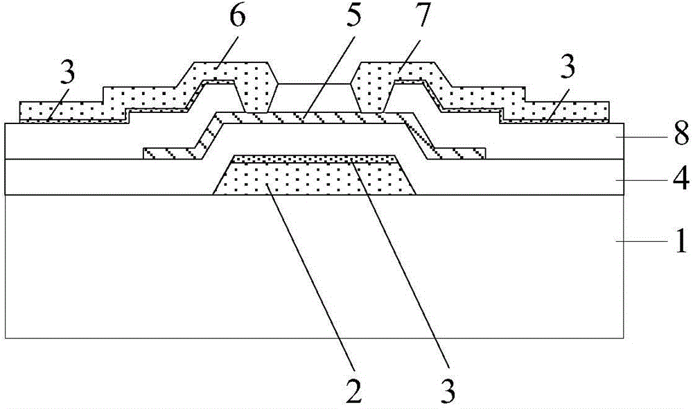
[0044] see image 3 The third thin film transistor provided by the embodiment of the present invention includes a base substrate 1, a gate electrode 2 formed of pure copper material, a gate insulating layer 4, an active layer 5, a source electrode 6, and a drain electrode 7. The thin film transistor also The copper alloy film layer 3 is included, and the copper alloy film layer 3 is arranged on the side of the gate electrode 2 facing the active layer 5 and on the sides of the source electrode 6 and the drain electrode 7 facing the active layer 5 . In this embodiment, a copper alloy film layer 3 is provided on the side of the gate electrode 2 of the thin film transistor facing the active layer 5, and the sides of the source electrode and the drain electrode facing the active layer, and the alloy elements in the copper alloy film layer 3 are in the crystal The accumulation at the boundaries, crystal planes, and surfaces can prevent the diffusion of copper atoms to the active lay...


PUM

PropertyMeasurementUnit
electrical resistivityaaaaaaaaaa

Abstract

The invention discloses a thin film transistor, a preparation method thereof, an array substrate and a display device. The thin film transistor, the preparation method thereof, the array substrate and the display device resolve the problems that an electrode or a wire made of Cu causes poor or abnormal display of the display device due to high diffusion capacity or easy oxidation. The thin film transistor comprises a grid electrode made of pure copper, a grid electrode insulation layer, an active layer, a source electrode, a drain electrode and a copper alloy film layer, wherein the copper alloy film layer is arranged on the surface, facing the active layer, of the grid electrode. The thin film transistor, the preparation method thereof, the array substrate and the display device have the advantages that the copper alloy film layer is arranged on the surface, facing the active layer, of the grid electrode of the thin film transistor, accumulation of alloy elements at the crystal boundary, the crystal surface and the surface can prevent diffusion of copper atoms towards the active layer, the oxidation resistance of the grid electrode is improved, and therefore the problem of poor or abnormal display of the display device caused when the thin film transistor fails or the display device has a Mura defect is avoided.

Description

technical field [0001] The invention relates to the field of display technology, in particular to a thin film transistor, a preparation method thereof, an array substrate and a display device. Background technique [0002] In the manufacturing process of the array substrate of the display device, Al is the earliest metal conductor material used. With the continuous improvement of the resolution of the display device, the aluminum material cannot meet the new requirements gradually. Among them, problems such as high resistivity, prone to electromigration failure, and formation of hillocks (Hillock) in the preparation process are the main shortcomings of the application of aluminum materials, especially with the improvement of the resolution of display devices, the density of wires and the average area The length of the wires has increased, so the aluminum material is no longer suitable for the preparation of the current display device. [0003] In order to solve the above pr...

Claims


Application Information

Patent Timeline
Patent Type & Authority Applications(China)
IPC IPC(8): H01L29/786H01L21/336H01L29/423H01L21/28
CPCH01L29/42384H01L27/124H01L27/1259H01L29/458H01L29/4908H01L29/786
Inventor 姜春生李旭远刘威朱夏明
Owner BOE TECH GRP CO LTD
Why Eureka
Try Eureka