

cr buffer circuit
A snubber circuit and current path technology, applied in circuit devices, emergency protection circuit devices, electrical components, etc., can solve the problems of large surge voltage and short-circuit damage of switching components, and achieve the effect of suppressing damping oscillation components and improving the reduction effect.
- Summary
- Abstract
- Description
- Claims
- Application Information
AI Technical Summary
Problems solved by technology
Method used
Image

Examples
Embodiment approach 1
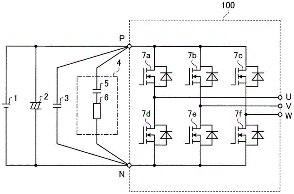
[0038] figure 1 It is a diagram showing a configuration example of a power semiconductor module employing the CR snubber circuit according to the first embodiment. exist figure 1 In the example shown, a power semiconductor module 100 is formed by full-bridge-connecting a plurality of switching elements 7a to 7f, and DC power is supplied from a DC power supply 1 connected between DC terminals P-N, and connected to an output terminal U. Three-phase AC power is supplied to unshown loads connected to , V, and W. In addition, the configuration of the power semiconductor module 100 is not limited thereto. For example, it may be formed by full-bridge connection of four switching elements, or may be formed by one or two switching elements, and the DC power supplied from the DC power supply 1 A configuration in which the voltage is lowered or boosted and supplied to the load, or a configuration in which AC power is supplied from the AC power supply instead of the DC power supply 1 ma...
Embodiment approach 2
[0052] Figure 9 It is a diagram showing an example of mounting the CR snubber circuit on the substrate according to the second embodiment. in addition, Figure 10 Indicates that the CR snubber circuit according to Embodiment 2 is mounted on the substrate, and Figure 9 Diagram of a different example. in addition, Figure 11 yes means Figure 9 and Figure 10 The equivalent circuit diagram of the CR snubber circuit is shown. Additionally, for Figure 9 The shown example of mounting the board on which the CR snubber circuit is mounted on the power semiconductor module is the same as that described in Embodiment 1. Figure 5 same, in addition, for Figure 10 The shown example of mounting the board on which the CR snubber circuit is mounted on the power semiconductor module is the same as that described in Embodiment 1. Figure 7 are the same, so the description is omitted here.
[0053] In Embodiment 1, an example in which surface mount capacitors and resistors are mou...
Embodiment approach 3
[0060] Figure 12 It is a diagram of an example of mounting the CR snubber circuit on the substrate according to the third embodiment. in addition, Figure 13 yes means Figure 12 The equivalent circuit diagram of the CR snubber circuit is shown. in addition, Figure 14 It is a diagram showing an example of the frequency characteristics of the CR snubber circuit according to the third embodiment. Additionally, for installations with Figure 12 The example of mounting the substrate of the CR snubber circuit shown in the power semiconductor module is the same as that described in Embodiment 1. Figure 5 are the same, so the description is omitted here.
[0061] In Embodiments 1 and 2, an example of changing the mounting position and number of resistors was described, but in Figure 12 In the example shown, it is formed so that, on one surface of the double-sided substrate 9 ( Figure 12 A plurality of capacitors 5a, 5b, 5c of the surface mount type can be mounted on the ...
PUM
 Abstract
Description
Claims
Application Information