Pixel circuit and driving method and application thereof
A technology of a pixel circuit and a driving method, applied in the field of display devices applying the pixel circuit, can solve the problems of inconsistent brightness of organic light emitting diodes, affecting the display effect of an active matrix organic light emitting display device, and inconsistent current of organic light emitting diodes, etc.
- Summary
- Abstract
- Description
- Claims
- Application Information
AI Technical Summary
Problems solved by technology
Method used
Image

Examples
Embodiment 1
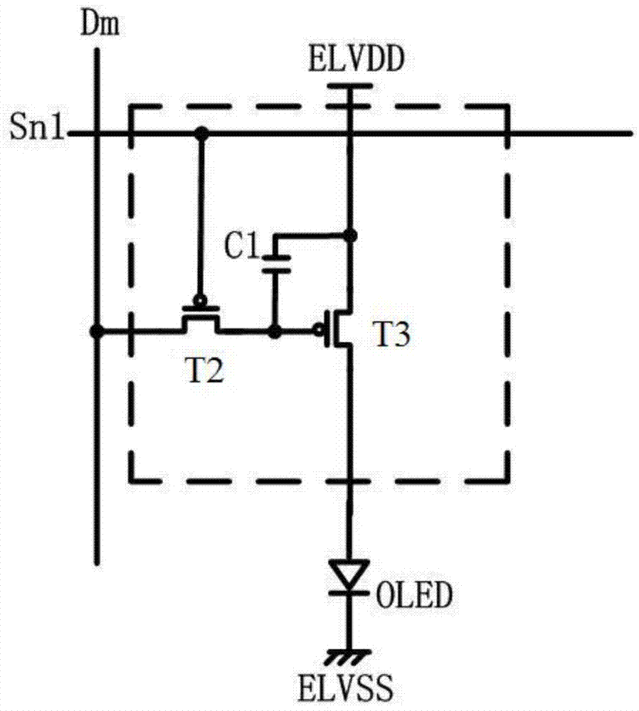
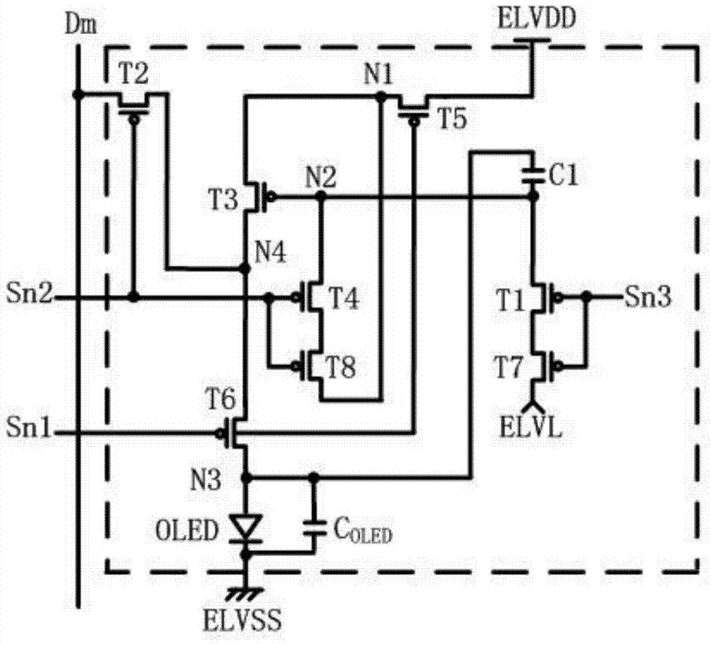
[0049] This embodiment provides a pixel circuit and its driving method, such as Figure 5 As shown, the pixel circuit is electrically connected to the data driver 130 through the data line Dm, and electrically connected to the scan driver 120 through the scan line Sni (i is 1, 2, 3); The initialization stage t1 of the control signal is initialized, the data model provided from the data line Dm is accepted in the programming stage t2, and the image is displayed by emitting light with a brightness corresponding to the data signal in the light-emitting stage t3; in the light-emitting stage t3, the scanning line Sni After being supplied, the scanning control signal transitions to an appropriate level, so as to supply current to the organic light emitting diodes provided in each pixel unit 110 .
[0050] Such as figure 2 As shown, each pixel circuit further includes a first power supply ELVDD and a second power supply ELVSS connected externally, and the first power supply ELVDD a...
Embodiment 2
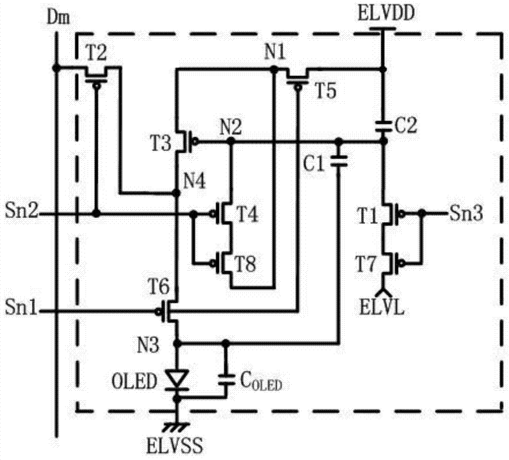
[0072] This embodiment provides a pixel circuit and its driving method, such as image 3 As shown, the pixel circuit and its driving method are the same as the first embodiment, the only difference is that the second capacitor C2 is electrically connected between the source of the fifth transistor T5 and the drain of the first transistor T1.
[0073] The plate of the second capacitor C2 electrically connected to the first transistor T1 is electrically connected to the second node N2, and the first capacitor C1 and the second capacitor C2 can simultaneously play the role of negative feedback of the anode voltage of the organic light emitting diode OLED, therefore, the The voltage fed back by the anode of the organic light emitting diode OLED is multiplied by the factor C1 / (C1+C2), so that the voltage fed back by the anode of the organic light emitting diode OLED can be controlled by setting the capacitance value of the second capacitor C2, which can be more The current flowing ...
Embodiment 3
[0075] This embodiment provides an active matrix organic light-emitting display device using the pixel circuit described in Embodiment 1, such as Figure 5 As shown, the active matrix organic light emitting display device in this embodiment includes: several pixel units 110 , a scan driver 120 and a data driver 130 . The pixel units 110 are arranged in a matrix at the intersection of the scan lines Sni and the data lines Dm, and are electrically connected to the data driver 130 through the data lines Dm, and electrically connected to the scan driver 120 through the scan lines Sni.
[0076] Each pixel unit 110 is initialized at the initialization stage t1 when the scan line Sni provides the scan control signal, and the pixel unit 110 receives the data signal provided from the data line Dm at the programming stage t2 when the scan control signal is provided by the scan line Sni; In the light-emitting phase t3, the scanning control signal provided by the scanning line Sn transiti...
PUM
 Abstract
Description
Claims
Application Information
 - R&D
- Intellectual Property
- Life Sciences
- Materials
- Tech Scout
- Unparalleled Data Quality
- Higher Quality Content
- 60% Fewer Hallucinations
Browse by: Latest US Patents, China's latest patents, Technical Efficacy Thesaurus, Application Domain, Technology Topic, Popular Technical Reports.
© 2025 PatSnap. All rights reserved.Legal|Privacy policy|Modern Slavery Act Transparency Statement|Sitemap|About US| Contact US: help@patsnap.com