Thin film transistor and manufacturing method thereof as well as array substrate and display device

A technology of thin-film transistors and doped layers, which is applied in the direction of transistors, semiconductor/solid-state device manufacturing, semiconductor devices, etc., can solve the problems of inability to reduce contact resistance, increase contact resistance, and current loss at the same time, so as to improve electron mobility and reduce Effect of contact resistance and reduction of current loss

Inactive Publication Date: 2015-06-17
BOE TECH GRP CO LTD +1
View PDF4 Cites 7 Cited by
  • Summary
  • Abstract
  • Description
  • Claims
  • Application Information

AI Technical Summary

Problems solved by technology

However, increasing the doping concentration of the dopant in the doped layer will increase the contact resistance between the doped layer and the active layer, which will also cause current loss.
That is, the existing technology cannot simultaneously reduce the contact resistance between the doped layer and the source / drain electrode layer and the contact resistance between the doped layer and the active layer, resulting in current loss

Method used


Image

  • Thin film transistor and manufacturing method thereof as well as array substrate and display device
  • Thin film transistor and manufacturing method thereof as well as array substrate and display device
  • Thin film transistor and manufacturing method thereof as well as array substrate and display device

Examples


Embodiment Construction

[0026] In order to further understand the technical solution of the present invention, the thin film transistor, the manufacturing method thereof, the array substrate, and the display device according to the embodiments of the present invention will be described in detail below with reference to the accompanying drawings.

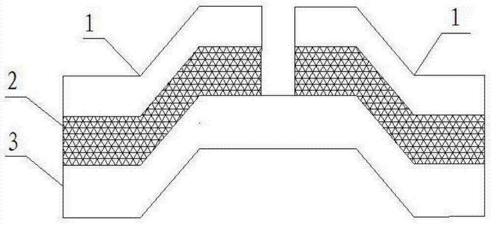
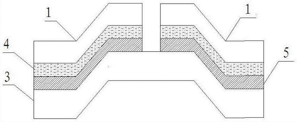
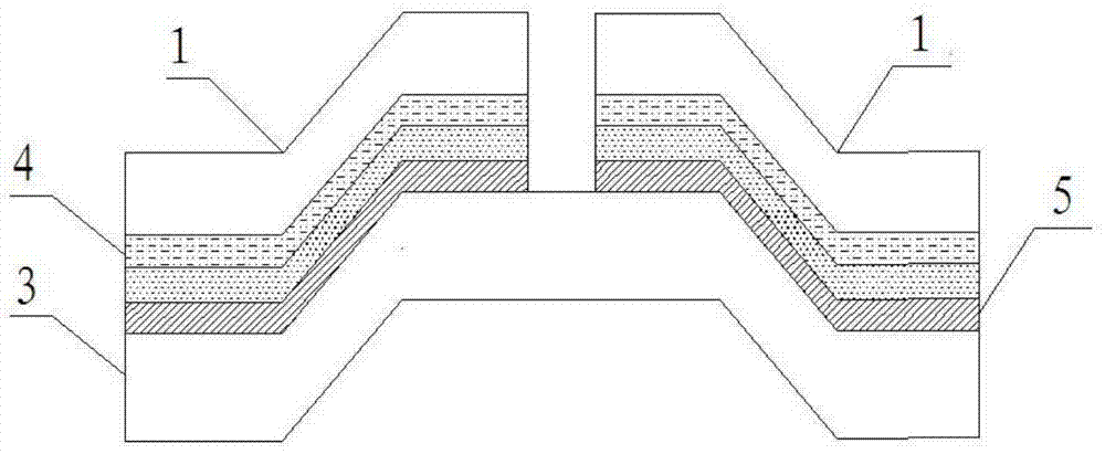
[0027] An embodiment of the present invention provides a thin film transistor, such as figure 2 A schematic cross-sectional view of the thin film transistor shown, which includes an active layer 3, a doped layer 2 and a source / drain electrode layer 1, and the doped layer 2 is located between the active layer 3 and the source / drain electrode layer 1 Among them, the doped layer 2 includes at least two sub-doped layers, and the doping concentration of the dopant in the source / drain sub-doped layer 4 close to the source / drain electrode layer 1 is higher than that close to the active sub-doped layer 1. The doping concentration of the dopant in the active sub-do...


PUM


Abstract

The invention relates to the display technology field, in particular to a thin film transistor and a manufacturing method thereof as well as an array substrate and a display device. The thin film transistor comprises an active layer (3), a doping layer (2) and a source / drain electrode layer (1), wherein the doping layer (2) is located between the active layer (3) and the source / drain electrode layer (1) and comprises at least two sub-doping layers, the doping concentration of dopant of the source / drain electrode sub-doping layer (4) close to the source / drain electrode layer (1) is larger than that of the dopant of an active sub-doping layer (5) close to the active layer (3), and the doping concentration of dopant of the active sub-doping layer (5) is larger than 0. According to the thin film transistor and the manufacturing method thereof as well as the array substrate and the display device, the technical problem that the contact resistance between the doping layer and the source / drain electrode layer and the contact resistance between the doping layer and the active layer cannot be reduced simultaneously in the prior art is solved, and the thin film transistor and the manufacturing method thereof as well as the array substrate and the display device can be applied to the display technology field.

Description

technical field [0001] The invention relates to the field of display technology, in particular to a thin film transistor and a preparation method thereof, an array substrate, and a display device. Background technique [0002] The main feature of a Thin Film Transistor Liquid Crystal Display (TFT-LCD) is that each pixel is equipped with a semiconductor switching device, that is, a Thin Film Transistor (TFT) device. A TFT device includes a gate electrode, a gate insulating layer, an active layer, and a source / drain electrode layer (including a source electrode, a drain electrode, and a channel) and the like. Among them, a metal-insulator-semiconductor (Metal Insulator Semiconductor, MIS) structure is formed between the gate electrode, the gate insulating layer, and the active layer, and the MIS structure is a key factor for the TFT device to be used as a switch. [0003] The electrical signal generated by the MIS structure in the TFT device is input and output from the sourc...

Claims


Application Information

Patent Timeline
IPC IPC(8): H01L29/786H01L29/45H01L21/336H01L21/28H01L27/12
Inventor 张首龙孙泉钦王丹名周唐臣李利芳张旗
Owner BOE TECH GRP CO LTD
Why Eureka
Try Eureka