
Method and apparatus for an active negative-capacitor circuit

A capacitor and negative capacitance technology, which is used in the field of active negative capacitor circuits and devices, can solve problems such as increased rebound and increased power loss

Inactive Publication Date: 2015-06-17
TENSORCOMM INC
View PDF7 Cites 4 Cited by
  • Summary
  • Abstract
  • Description
  • Claims
  • Application Information

AI Technical Summary

Problems solved by technology

However, larger transistors (in addition to increasing bounce and power loss) also increase the delay in signal transfer due to the larger gate capacitance presented to the output of the PGA

Method used


Image

  • Method and apparatus for an active negative-capacitor circuit
  • Method and apparatus for an active negative-capacitor circuit
  • Method and apparatus for an active negative-capacitor circuit

Examples


Embodiment Construction

[0040] The invention described in this specification can be used in any wired or wireless system or any low supply voltage design. These techniques can be used for any amplifier design, ADC design, or PGA and ADC interface design. These techniques can be extended to other circuit designs where increased bandwidth between two interfaces, reduced clock bounce, or matched transistors within the circuit are desired.

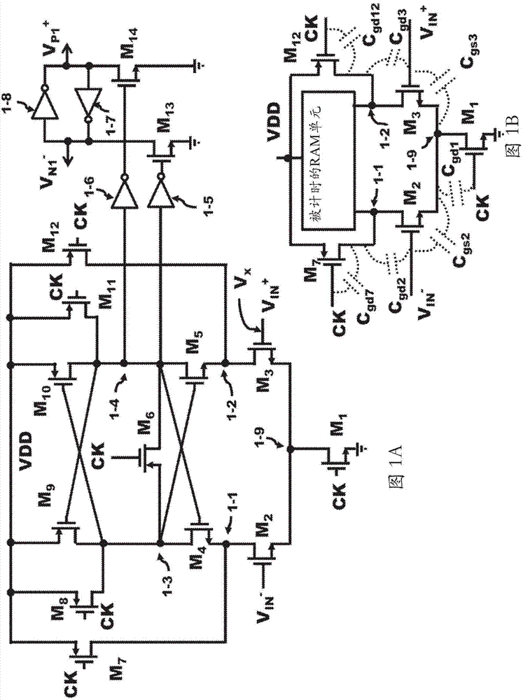
[0041] Figure 1A The comparator clocked in the first preamplifier stage is shown in . The basic construction of a clocked preamplifier stage includes a ground switch M 1 , the ground switch has a gate coupled to a clock CK. m 1 The drains 1-9 are coupled to two N-channel transistors M 2 and M 3 source. m 2 by V IN - driven while M 3 by another differential input signal V IN+ driven by. m 2 The drain of is coupled to 1-1 and is also coupled to a P-channel transistor M controlled by the same clock CK 7 the drain. m 3 The drains 1-2 of are coupled to a ...


PUM


Abstract

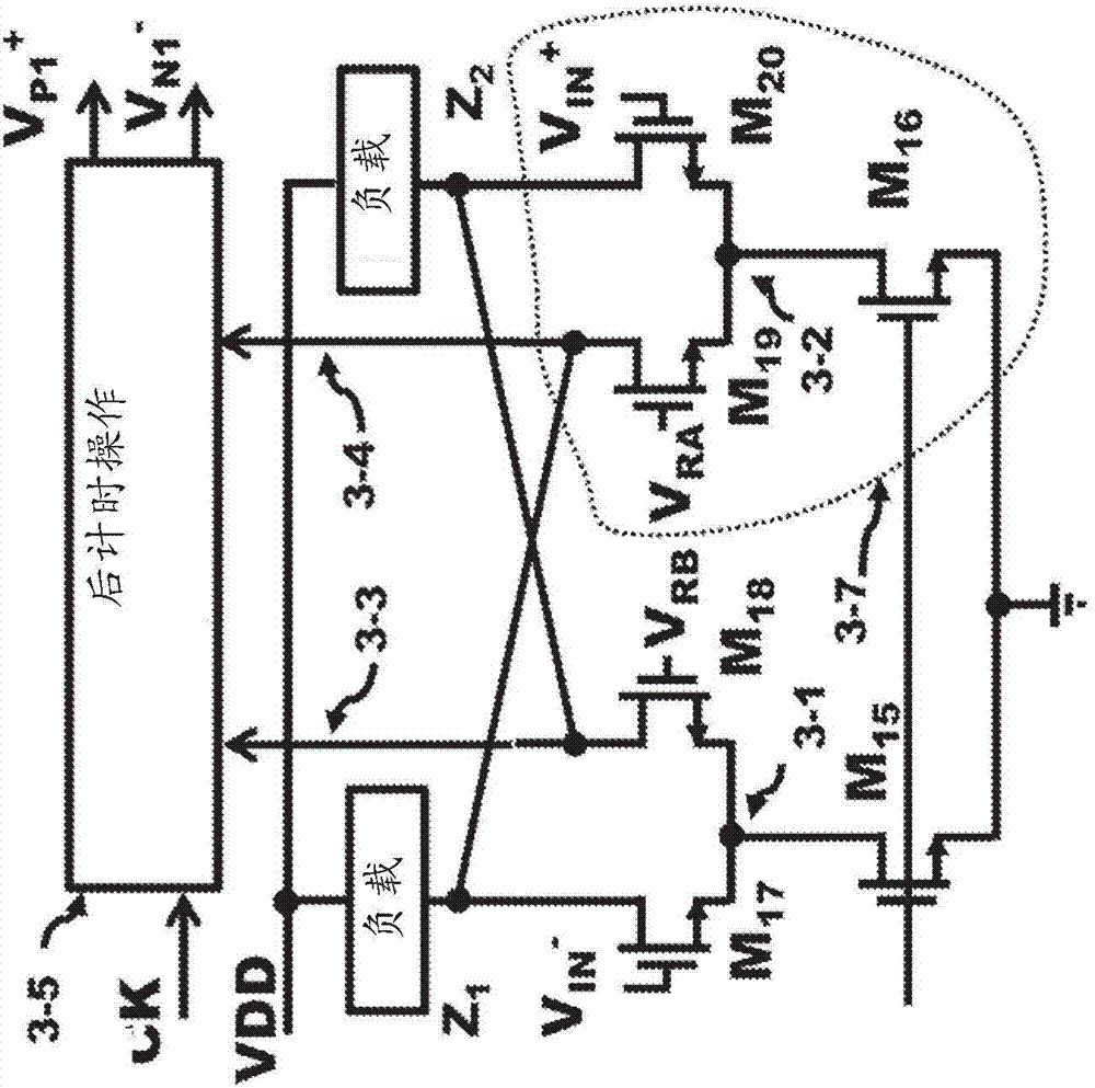
The differential output of a Programmable Gain Amplifier (PGA) is loaded by the input differential gate capacitance of a plurality of Analog to Digital convertors (ADC) comparators and the differential metal layer traces to interconnect these comparators to the PGA. The differential capacitive load presented to the PGA is quite large and reduces the bandwidth of this interconnect between the PGA and ADC. To overcome the performance degradation due to the differential capacitive load, an active negative-capacitor circuit cancels the effect of the large input capacitance of the ADC comparators. This cancelation extends the gain characteristics of the interconnect between the PGA's output and the inputs of the first stage of the comparators. The active negative-capacitance is comprised of a cross pair NMOS with a capacitor connecting their sources where each NMOS is biased by a current source.

Description

[0001] Cross References to Related Applications [0002] The title of this application on September 3, 2012 is "Method and Apparatus for an Active Negative-Capacitor Circuit to Cancel the input Capacitance of Comparators for an Active Negative-Capacitor Circuit to Cancel the Input Capacitance of Comparators" 13 / 602,216 of earlier US Application No. 13 / 602,216 of ". This application is submitted on September 3, 2012 and is entitled "Method and Apparatus for Reducing the Clock Kick-Back of ADC Comparators While Maintaining Transistor Matching Behavior and Reducing the Clock Kick-Back of ADC Comparators While Maintaining Transistor Matching Behavior)" by the same inventor as this application and incorporated herein by reference in its entirety. Background technique [0003] The Federal Communications Commission (FCC) has allocated bandwidth spectrum in the 60GHz frequency range (57GHz to 64GHz). The goal of the Wireless Gigabit Alliance (WiGig) is to standardize this frequency ...

Claims


Application Information

Patent Timeline
Patent Type & Authority Applications(China)
IPC IPC(8): H03F3/45
CPCH03M1/0818H03M1/0809H03M1/124H03M1/365
Inventor 岱·戴
Owner TENSORCOMM INC
Learn More