ADS array substrate, manufacturing method thereof, and display device comprising same

The technology of an array substrate and a manufacturing method, which is applied in the field of liquid crystal display, can solve the problems of common electrode signal distortion and green screen, and achieve the effects of reducing coupling capacitance, reducing resistance, and improving signal distortion problems

Inactive Publication Date: 2015-06-24
BOE TECH GRP CO LTD +1
View PDF5 Cites 11 Cited by
  • Summary
  • Abstract
  • Description
  • Claims
  • Application Information

AI Technical Summary

Problems solved by technology

[0005] The present invention provides an ADS array substrate and a manufacturing method thereof, which are used to solve the problem of greening of the screen due to serious distortion of the common electrode signal

Method used


Image

  • ADS array substrate, manufacturing method thereof, and display device comprising same
  • ADS array substrate, manufacturing method thereof, and display device comprising same
  • ADS array substrate, manufacturing method thereof, and display device comprising same

Examples


Embodiment Construction

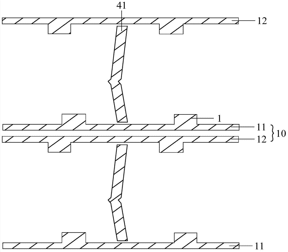
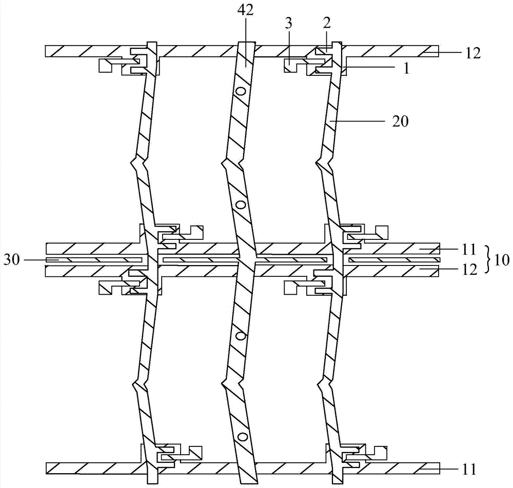
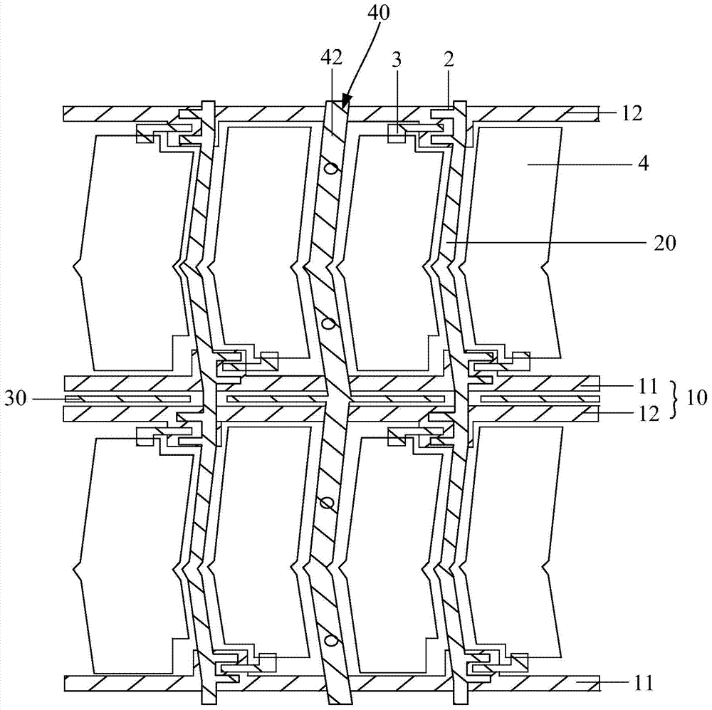
[0037] The invention provides an ADS array substrate and a manufacturing method thereof, which are used to solve the problem that the common electrode causes level drift and serious signal distortion due to coupling capacitance, which causes the screen to turn green.

[0038] The ADS array substrate includes a common electrode and a plurality of sub-pixel regions, a metal line is arranged between at least partially adjacent two sub-pixel regions, and the metal line is connected in parallel with the common electrode to reduce the resistance of the common electrode, Therefore, the coupling capacitance of the common electrode can be reduced, the problems of level drift and signal distortion of the common electrode can be improved, the phenomenon of greening of the picture is greatly improved, and the picture display quality of the display device is improved.

[0039] Wherein, the sub-pixel area is defined by the gate line and the data line, and the coupling capacitance is mainly g...


PUM


Abstract

The invention relate to the technical field of liquid crystal display, and discloses an ADS array substrate, a manufacturing method thereof and a display device comprising the same. The ADS array substrate comprises a pixel electrode and a common electrode. A metal line is arranged between at least two adjacent sub pixel areas, and the metal line is connected with the common electrode in parallel, so that the resistance of the common electrode is reduced, the coupling capacitance of the common electrode can be reduced, the problems of level drifting and signal distortion of the common electrode are solved, and the phenomenon of picture yellow discolouration is greatly reduced. The display device comprises the ADS array substrate. The display quality of the pictures is improved.

Description

technical field [0001] The invention relates to the technical field of liquid crystal display, in particular to an ADS array substrate, a manufacturing method thereof, and a display device. Background technique [0002] Thin Film Transistor-Liquid Crystal Display (TFT-LCD) has the characteristics of small size, low power consumption, and no radiation. It has developed rapidly in recent years and occupies a dominant position in the current flat panel display market. The main structure of TFT-LCD is a liquid crystal panel. The liquid crystal panel includes a thin film transistor array substrate and a color filter substrate in a box, and liquid crystal molecules are filled between the array substrate and the color filter substrate. The liquid crystal panel controls the common electrode and the pixel electrode to form an electric field that drives the deflection of the liquid crystal molecules to realize gray scale display. The filter layer on the color filter substrate is used...

Claims


Application Information

Patent Timeline
Patent Type & Authority Applications(China)
IPC IPC(8): G02F1/1343G02F1/1333
CPCG02F1/134309G02F1/136286G02F1/1368G02F2201/121G02F2201/123G02F1/13629
Inventor 王骁
Owner BOE TECH GRP CO LTD
Why Eureka
Try Eureka