Semiconductor device and forming method thereof

A semiconductor and device technology, applied in the field of semiconductor devices and their formation, can solve the problems of small metal gate height and other problems

Inactive Publication Date: 2015-06-24
SEMICON MFG INT (SHANGHAI) CORP
View PDF3 Cites 2 Cited by
  • Summary
  • Abstract
  • Description
  • Claims
  • Application Information

AI Technical Summary

Problems solved by technology

Therefore, if the interlayer dielectric layer is consumed too much,

Method used


Image

  • Semiconductor device and forming method thereof
  • Semiconductor device and forming method thereof
  • Semiconductor device and forming method thereof

Examples


Embodiment Construction

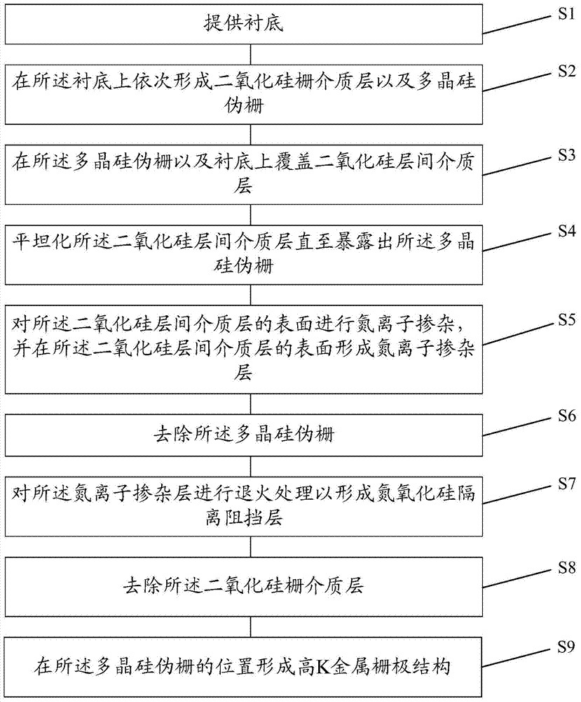
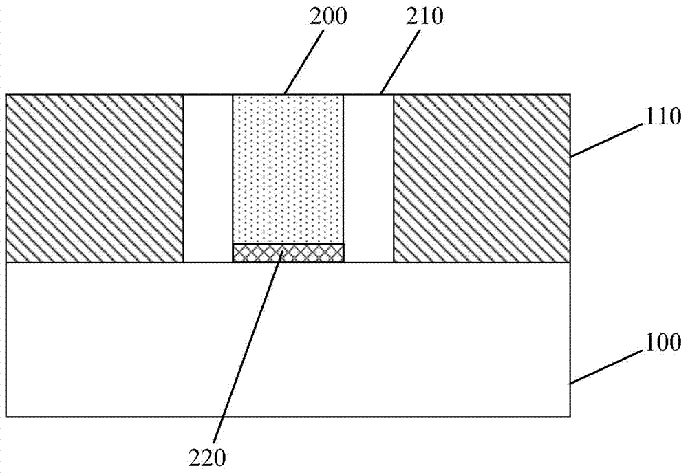
[0047] In the existing gate-last process, it is easy to affect the interlayer dielectric layer during the process of removing the dummy gate. The reason is that a relatively dense gate dielectric layer is formed at the bottom of the dummy gate, and when the dummy gate is removed, the gate dielectric layer also needs to be removed. In the process of removing the gate dielectric layer, the surface of the interlayer dielectric layer is easily consumed (loss) to a certain extent, so that the height of the interlayer dielectric layer becomes lower. The reduction in the height of the interlayer dielectric layer results in a corresponding reduction in the height of the subsequently formed gate.

[0048] In order to solve the technical problem, the present invention provides a method for forming a semiconductor device, performing ion doping on the surface of the interlayer dielectric layer to form a doped layer on the surface of the interlayer dielectric layer, the doping The layer c...


PUM


Abstract

A semiconductor device forming method comprises steps: a substrate is provided, and a gate dielectric layer and a pseudo gate; an interlayer dielectric layer flush with the pseudo gate is formed on the substrate; ion doping is carried out on the surface of the interlayer dielectric layer so as to form a doping layer on the surface of the interlayer dielectric layer; the gate dielectric layer and the pseudo gate are removed; and a gate electrode structure is formed at the pseudo gate position. The invention also provides a semiconductor device, which comprises the substrate, the gate electrode, the interlayer dielectric layer and an isolation layer arranged on the surface of the interlayer dielectric layer. The semiconductor device and the forming method thereof have the beneficial effects that through carrying out ion doping on the surface of the interlayer dielectric layer and the surface of the exposed pseudo gate and forming the doping layers on the surface of the interlayer dielectric layer and the surface of the pseudo gate, the doping layers can well block influences on the interlayer dielectric layer by the subsequent pseudo gate removal step, surface losses of the interlayer dielectric layer are further reduced, and the height of the gate electrode formed subsequently can be ensured.

Description

technical field [0001] The invention relates to the field of semiconductor manufacturing, in particular to a semiconductor device and a forming method thereof. Background technique [0002] In the existing gate-last process (gate-last), usually a gate dielectric layer and a dummy gate are first formed on a substrate, and semiconductor devices such as a source region and a drain region are formed accordingly. After that, an interlayer dielectric (inter layer dielectric, ILD) is formed on these semiconductor devices, and the dummy gate is removed to form an opening, and finally a metal gate is formed in the opening. [0003] Since the dummy gate needs to be removed and a metal gate is formed at the position of the dummy gate, the process of removing the dummy gate and the gate dielectric layer is likely to affect the interlayer dielectric layer, resulting in the A certain degree of consumption (loss) occurs on the surface of the interlayer dielectric layer. [0004] Since th...

Claims


Application Information

Patent Timeline
IPC IPC(8): H01L21/28H01L29/423
Inventor 陈勇卜伟海
Owner SEMICON MFG INT (SHANGHAI) CORP
Why Eureka
Try Eureka