Mask for reflection type photolithography technology and manufacture method and using method thereof

A photolithography technology and mask technology, which is applied to the originals for photomechanical processing, microlithography exposure equipment, photolithography process of pattern surface, etc. It can solve problems such as affecting the accuracy of patterns and avoid shadow effects. , high reflectivity, clear interface effect

Active Publication Date: 2015-07-01
SEMICON MFG INT (SHANGHAI) CORP
View PDF4 Cites 10 Cited by
  • Summary
  • Abstract
  • Description
  • Claims
  • Application Information

AI Technical Summary

Problems solved by technology

As a result, shadowing effects can be produced, affecting the accuracy of the final pattern

Method used


Image

  • Mask for reflection type photolithography technology and manufacture method and using method thereof
  • Mask for reflection type photolithography technology and manufacture method and using method thereof
  • Mask for reflection type photolithography technology and manufacture method and using method thereof

Examples


Embodiment Construction

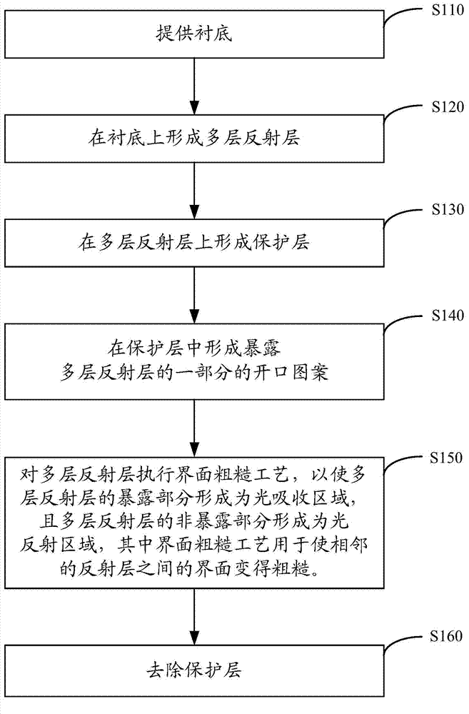
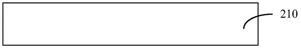
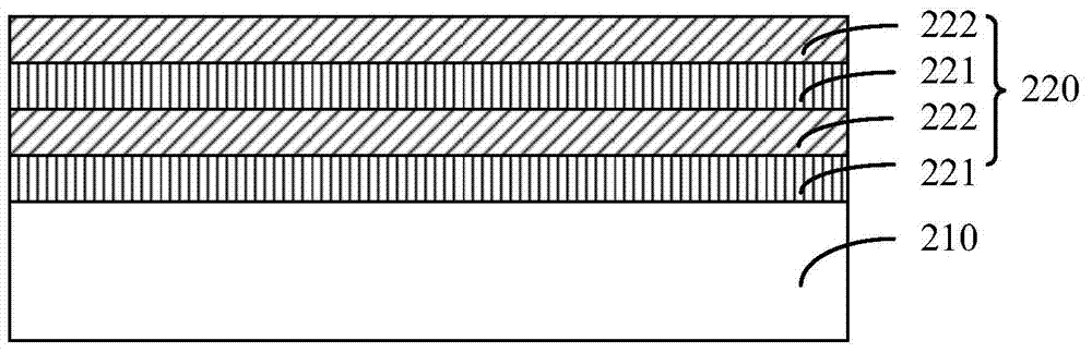
[0020] Next, the present invention will be described more fully with reference to the accompanying drawings, in which embodiments of the invention are shown. However, this invention may be embodied in different forms and should not be construed as limited to the embodiments set forth herein. Rather, these embodiments are provided so that this disclosure will be thorough and complete, and will fully convey the scope of the invention to those skilled in the art. In the drawings, the size and relative sizes of layers and regions may be exaggerated for clarity. Like reference numerals refer to like elements throughout.

[0021] It will be understood that when an element or layer is referred to as being "on," "adjacent," "connected to" or "coupled to" another element or layer, it can be directly on the other element or layer. A layer may be on, adjacent to, connected to, or coupled to other elements or layers, or intervening elements or layers may be present. In contrast, when a...


PUM

PropertyMeasurementUnit
interface roughnessaaaaaaaaaa
thicknessaaaaaaaaaa
thicknessaaaaaaaaaa

Abstract

The invention discloses a mask for the reflection type photolithography technology and a manufacture method and a using method of the mask. The method for manufacturing the mask for the reflection type photolithography technology comprises the following steps: providing a substrate; forming multiple reflecting layers on the substrate; forming protecting layers on the multiple reflecting layers; forming opening patterns exposing one part of each reflecting layer in the protecting layers; carrying out interface roughing process on the multiple reflecting layers and enabling the exposure parts of the multiple reflecting layers to form light absorption areas and enabling the non-exposed parts of the multiple reflecting layers to form light reflection areas, wherein the interface roughing process is used for roughing the interfaces of adjacent reflecting layers; and removing the protecting layer. According to the mask for the reflection type photolithography technology, manufactured by the method, no height difference exists between the light reflecting area and the light absorption area, light reflected by the light reflecting area cannot be absorbed by the light absorption area and the shadow effect can be avoided.

Description

technical field [0001] The invention relates to the technical field of semiconductors, in particular to a reticle for reflective photolithography, a manufacturing method and a using method thereof. Background technique [0002] Photolithography is a commonly used technology in the field of semiconductor technology at present. In photolithography, the exposure process usually requires the use of a mask. The traditional reticle is a transmissive reticle, and visible light or ultraviolet light passes through the reticle to expose the photoresist. However, with the continuous development of semiconductor technology, the size of semiconductor devices is continuously reduced. Traditional visible light or ultraviolet light can no longer meet the requirements of pattern resolution. Therefore, exposure with shorter wavelength light such as extreme ultraviolet EUV is required. Since EUV light is easily absorbed by all substances, it is not possible to expose with a traditional tra...

Claims


Application Information

Patent Timeline
Patent Type & Authority Applications(China)
IPC IPC(8): G03F1/24G03F7/20
Inventor 徐垚
Owner SEMICON MFG INT (SHANGHAI) CORP
Why Eureka
Try Eureka