Optical proximity correction method

An optical proximity correction and photon technology, which is applied in optics, microlithography exposure equipment, and originals for photomechanical processing, can solve problems such as deviation and semiconductor device performance, and achieve the effect of reducing the change of overlapping area

Active Publication Date: 2015-07-01
SEMICON MFG INT (SHANGHAI) CORP
View PDF8 Cites 9 Cited by
  • Summary
  • Abstract
  • Description
  • Claims
  • Application Information

AI Technical Summary

Problems solved by technology

[0007] However, the change of the size of the exposure target pattern will cause a certain deviation between the size of the etched pattern formed by subsequent etching using the patterned photoresist layer as a mask and the design size, which may affect the final semiconductor device. performance impact

Method used


Image

  • Optical proximity correction method
  • Optical proximity correction method
  • Optical proximity correction method

Examples


Embodiment Construction

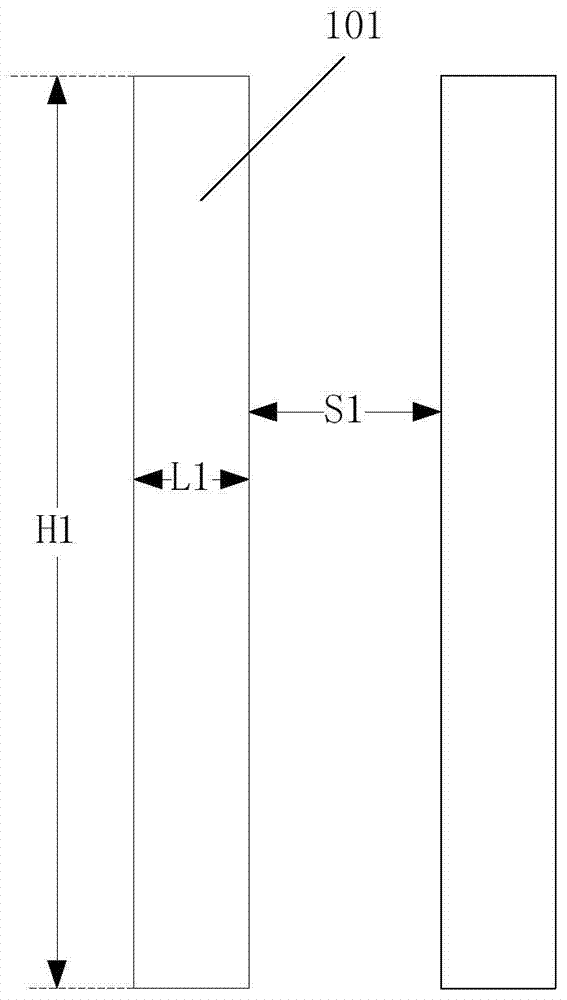
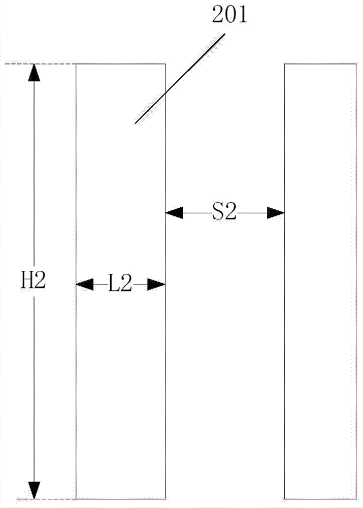
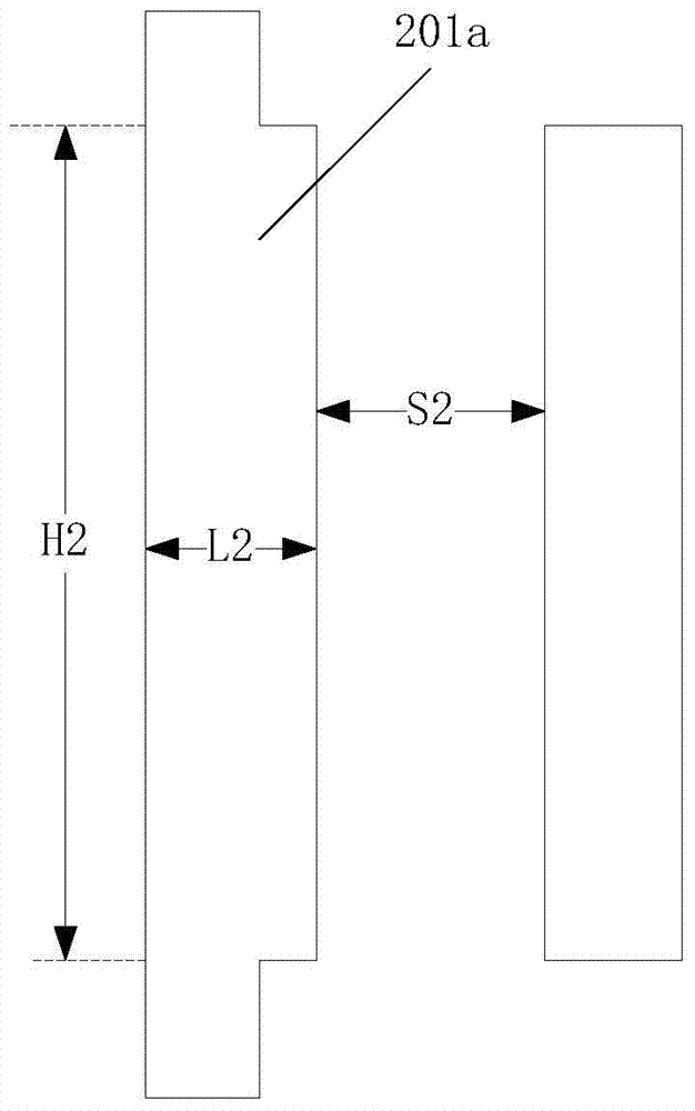
[0035] As described in the background technology, by changing the width of the exposure target pattern, the exposure target pattern is changed from an unexposed pattern to an exposed pattern, resulting in the size of the material layer to be etched corresponding to the exposure target pattern after being etched. There is a certain deviation from the design size, which may affect the performance of the semiconductor device in the chip.

[0036] Research has found that in the process of forming a polysilicon gate with a polysilicon layer as an etching material layer, reducing the width of the exposure target for etching the polysilicon layer will reduce the width of the finally formed polysilicon gate, thereby causing the polysilicon gate The channel width of the transistor where it is located is reduced, which affects the electrical parameters such as the saturation current of the transistor and affects the performance of the transistor; and the metal plug that should have been ...


PUM

PropertyMeasurementUnit
widthaaaaaaaaaa
lengthaaaaaaaaaa
lengthaaaaaaaaaa

Abstract

The invention discloses an optical proximity correction method which is as follows: a photolithographic resolution limit table is established, and the photolithographic resolution limit table includes an exposable area and a non-exposable area; current layer and adjacent layer graphs are provided, and the current layer and adjacent layer graphs are overlapped to form an overlapping graph; a bad edge of the current layer graph is determined; cut-off points are added into the bad edge, the cut-off points are respectively located below or above a first adjacent layer sub graph, the bad edge part between the cut-off points is used as a first line segment, other bad edge part is used as a second line segment, and the second line segment is moved, so that a second width is formed between a second line segment relative edge in a first to-be-detected sub graph and the second line segment, a second distance is formed between the second line segment and an adjacent current layer sub graph, and the second width and the second distance are located in the exposable area in the photolithographic resolution limit table; and according to the length of the first line segment, the first line segment can be moved a corresponding distance. The influence on semiconductor device performances can be avoided.

Description

technical field [0001] The invention relates to the technical field of semiconductors, in particular to an optical proximity correction method. Background technique [0002] Photolithography technology is a crucial technology in semiconductor manufacturing technology, which can realize the transfer of patterns from the mask to the surface of silicon wafers to form semiconductor products that meet the design requirements. In the photolithography process, first, through the exposure step, the light is irradiated on the silicon wafer coated with photoresist through the light-transmitting area of ​​the mask plate, and reacts photochemically with the photoresist; then, through the development step, Using the degree of dissolution of the photosensitive and unphotosensitive photoresist to the developer, a photolithographic pattern is formed to realize the transfer of the mask pattern; then, through the etching step, the silicon wafer is etched based on the pattern formed by the pho...

Claims


Application Information

Patent Timeline
Patent Type & Authority Applications(China)
IPC IPC(8): G03F7/20G03F1/36
Inventor 王铁柱
Owner SEMICON MFG INT (SHANGHAI) CORP
Why Eureka
Try Eureka