
Method for forming fin field effect transistor

A fin field effect and transistor technology, which is applied in semiconductor devices, semiconductor/solid-state device manufacturing, electrical components, etc., and can solve problems such as poor performance of fin field effect transistors

Active Publication Date: 2017-11-03
SEMICON MFG INT (SHANGHAI) CORP
View PDF3 Cites 0 Cited by
  • Summary
  • Abstract
  • Description
  • Claims
  • Application Information

AI Technical Summary

Problems solved by technology

[0010] The problem solved by the present invention is the poor performance of fin field effect transistors in the prior art

Method used


Image

  • Method for forming fin field effect transistor
  • Method for forming fin field effect transistor
  • Method for forming fin field effect transistor

Examples


Embodiment Construction

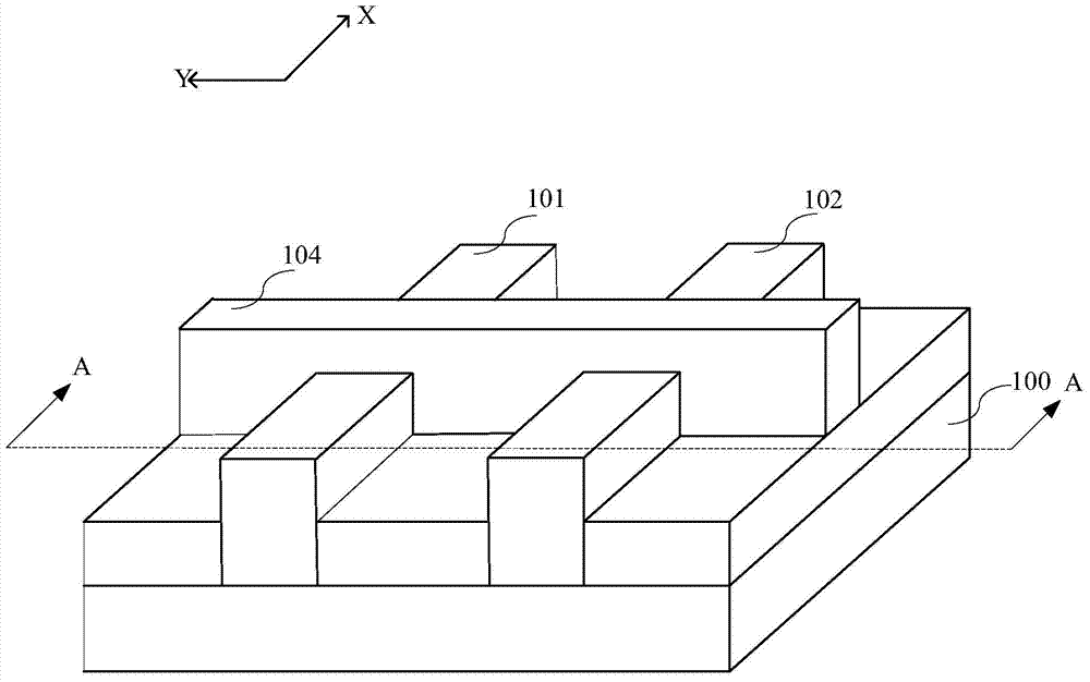
[0044] refer to figure 1 If ion implantation is directly performed on the first fins 101 on both sides of the gate 104, the ion implantation process will make most of the single crystal silicon in the first fins 101 be converted into amorphous silicon. Compared with single crystal silicon, the grain size of amorphous silicon is not uniform, and the arrangement is disorderly. Therefore, the resistance value of the first fin portion 101 composed of amorphous silicon is relatively large. In addition, it is difficult to determine the resistance or other physical properties of the first fin portion 101 composed of amorphous silicon, so that it is difficult to control the overall physical properties of the subsequently formed FinFET.

[0045]In the process of forming the first fin field effect transistor, a patterned amorphous carbon layer is formed on the substrate, exposing the first fin portion 101 and the gate thereon. Next, the substrate is heated, and high-temperature ion imp...


PUM


Abstract

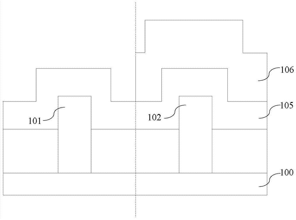
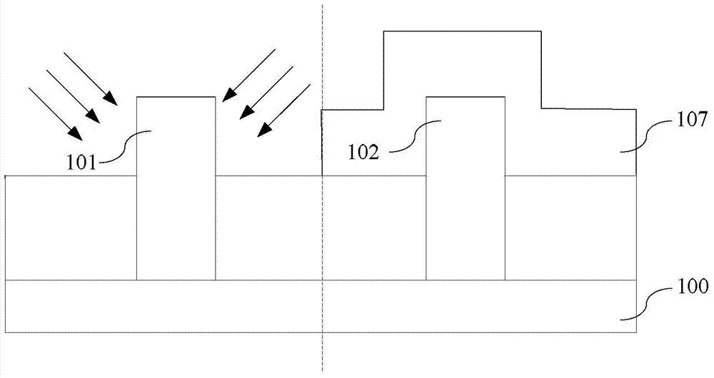
A forming method of a fin type field effect transistor comprises the following steps: forming adjacent first fin portion and second fin portion on a substrate; forming a grid electrode spanning the first fin portion and the second fin portion; sequentially forming a first protective layer, a first etching stop layer, a second protective layer and a second etching stop layer covering the grid electrode and the substrate from top to bottom; forming a patterned mask layer on the second etching stop layer, wherein the patterned mask layer covers the second etching stop layer of the second fin portion; removing the second etching stop layer on the first fin portion, then removing the patterned mask layer and the second protective layer on the first fin portion in a same technology; removing the first etching stop layer on the first fin portion by a first etching, then removing the first protective layer on the first fin portion by a second etching to expose the first fin portion; heating the substrate, injecting ions into the first fin portion on bilateral sides of the grid electrode to form a source electrode and a drain electrode; removing the first etching stop layer and the first protective layer covering the second fin portion. By the method of the fin type field effect transistor, the difficulty in manufacturing the transistor is reduced, and the performance of the transistor is improved.

Description

technical field [0001] The invention relates to the field of semiconductors, in particular to a method for forming a fin field effect transistor. Background technique [0002] With the development of the semiconductor industry to lower technology nodes, the transition from planar CMOS transistors to three-dimensional FinFET (3D Fin Field Effect Transistor) device structures has gradually begun. In FinFET, the gate structure can control the channel from at least two sides, which has a much stronger control ability of the gate to the channel than planar MOSFET devices, and can well suppress the short channel effect. And compared with other devices, it has better compatibility with the existing integrated circuit production technology. [0003] The forming method of the fin field effect transistor in the prior art is as follows: [0004] refer to figure 1 , providing a semiconductor substrate 100 with raised first fins 101 and second fins 102 on the substrate 100 . The firs...

Claims


Application Information

Patent Timeline
Patent Type & Authority Patents(China)
IPC IPC(8): H01L21/336H01L21/28H01L21/8238
CPCH01L21/28H01L29/06H01L29/66795
Inventor 何其暘张翼英
Owner SEMICON MFG INT (SHANGHAI) CORP
Learn More