Laser annealing device and method
A technology of laser annealing and laser beam, which is applied in the direction of laser welding equipment, electrical components, circuits, etc., can solve the problems that the uniformity of annealing, the size of the beam cannot be guaranteed, and the energy density of annealing cannot be guaranteed, so as to save time, The effect of improving efficiency and ensuring the uniformity of annealing
- Summary
- Abstract
- Description
- Claims
- Application Information
AI Technical Summary
Problems solved by technology
Method used
Image
Examples
Embodiment 1
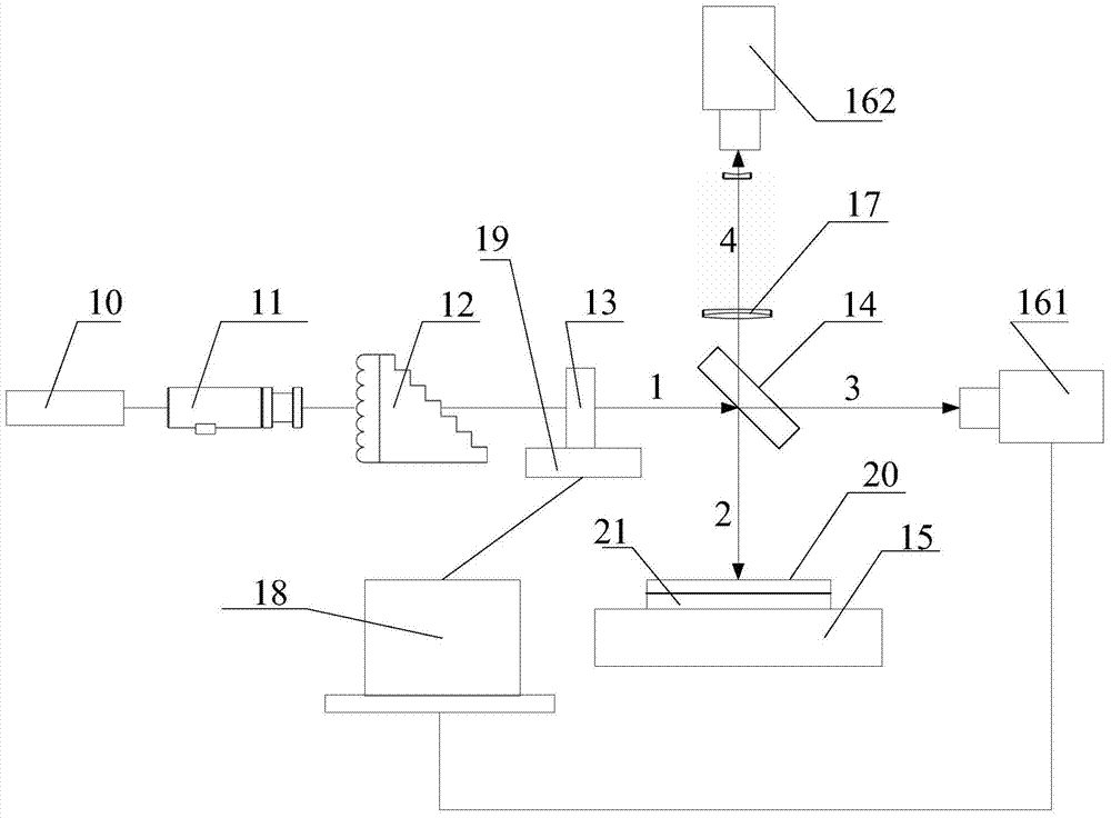
[0033] Please refer to figure 1 , a laser annealing device, comprising: a solid-state laser light source 10, providing a laser beam;
[0034] The scanning unit 15 supports the substrate 21, and scans the semiconductor film 20 on the support substrate 21 with the laser beam in the direction of the short axis of the laser beam, and anneals the semiconductor film 20 by laser irradiation. ;
[0035] Also includes a beam expander unit 11: used to expand the size of the laser beam;
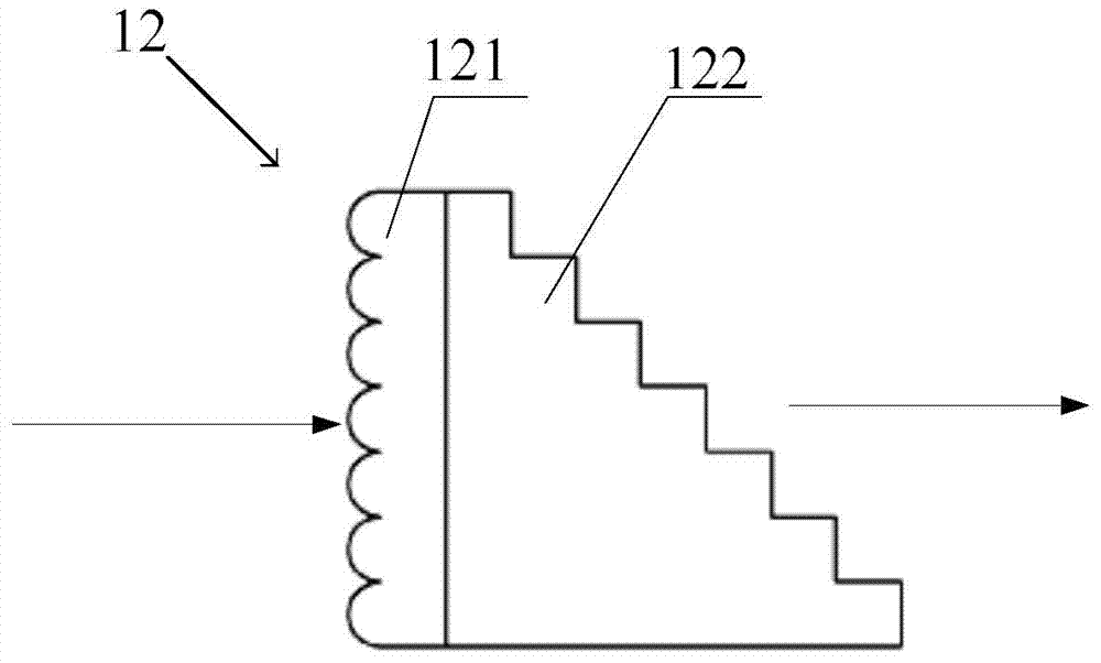
[0036] Homogenizing unit 12, used to reduce the interference effect of the laser beam; said homogenizing unit 12 includes a cylindrical surface 121 and a step-shaped cylindrical mirror 122, and said cylindrical surface 121 is arranged near the beam expanding unit 11 At one end, the cylindrical mirror 122 is disposed at the end far away from the beam expander unit 11 .
[0037]The cylindrical surface 121 is narrow, similar to a microlens, and can be completed by etching; the stepped cylindrical mirror...
Embodiment 2
[0053] A method for laser annealing, comprising the following steps: Step 1: start the solid-state laser light source 10 to emit a laser beam; The above-mentioned laser beam is shaped; Step 3, the outgoing light from the condenser lens unit 13 is projected onto the surface of the semiconductor film 20 and the first beam detector 161 by the spectroscopic unit 14; Step 4: Use the scanning unit 15 to The laser beam scans the semiconductor film 20 relatively in the short axis direction of the laser beam, so that the laser irradiation anneals the semiconductor film 20; step five: monitor the transmission of the light splitting unit 14 through the first beam detector 161 The size of the light, that is, the third incident light changes in size to monitor the change in the size of the laser spot irradiated on the surface of the semiconductor film 20 .
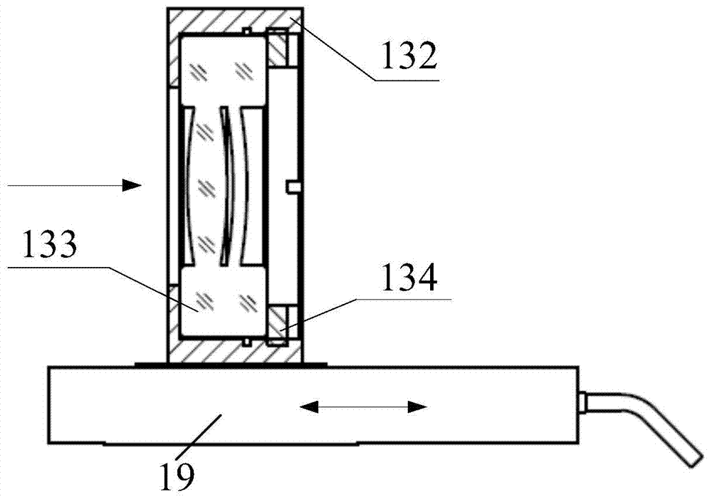
[0054] Preferably, the position of the focusing lens unit is adjusted based on the value of the spot size monitored in step five, so ...
PUM
 Abstract
Description
Claims
Application Information
 - R&D Engineer
- R&D Manager
- IP Professional
- Industry Leading Data Capabilities
- Powerful AI technology
- Patent DNA Extraction
Browse by: Latest US Patents, China's latest patents, Technical Efficacy Thesaurus, Application Domain, Technology Topic, Popular Technical Reports.
© 2024 PatSnap. All rights reserved.Legal|Privacy policy|Modern Slavery Act Transparency Statement|Sitemap|About US| Contact US: help@patsnap.com


