Semiconductor device and method for forming same, method for improving wafer dicing yield

A semiconductor and yield technology, applied in the direction of semiconductor devices, semiconductor/solid-state device manufacturing, semiconductor/solid-state device components, etc., can solve the problem of chip performance and service life decline, chips are easily damaged, and wafer cutting yield is low, etc. problems, to achieve the effect of improving wafer cutting yield and good interconnection performance

Active Publication Date: 2017-12-29
SEMICON MFG INT (SHANGHAI) CORP
View PDF3 Cites 0 Cited by
  • Summary
  • Abstract
  • Description
  • Claims
  • Application Information

AI Technical Summary

Problems solved by technology

This will cause the loss of the protective effect of the sealing ring, the chip is easily damaged in the packaging structure, and the performance and service life of the chip will be reduced
In addition, if the crack extends into the chip, it will destroy the interconnection structure, the plug layer in the interconnection structure will break, and the signal transmission channel in the interconnection structure will be disconnected, causing the chip to fail, for example, some functions of the chip cannot work normally. Or the performance of the chip does not meet the design requirements
That is, the existing wafer cutting yield is low

Method used


Image

  • Semiconductor device and method for forming same, method for improving wafer dicing yield
  • Semiconductor device and method for forming same, method for improving wafer dicing yield
  • Semiconductor device and method for forming same, method for improving wafer dicing yield

Examples


Embodiment Construction

[0040] In order to make the above objects, features and advantages of the present invention more comprehensible, specific embodiments of the present invention will be described in detail below in conjunction with the accompanying drawings.

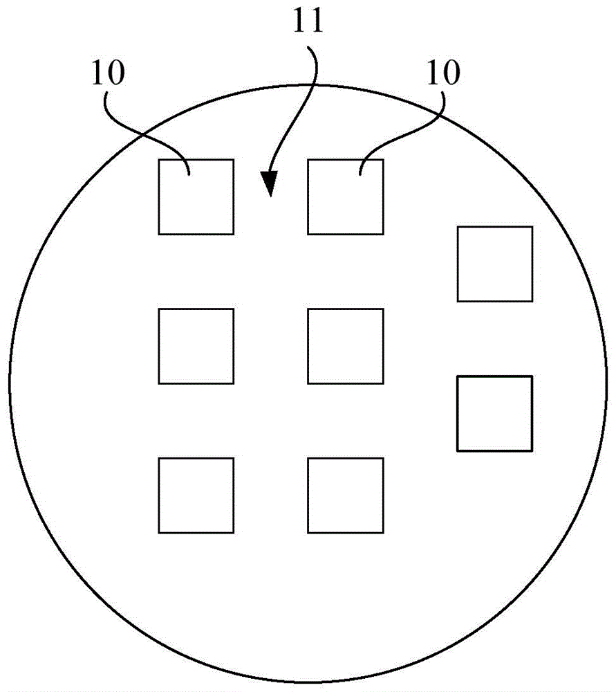
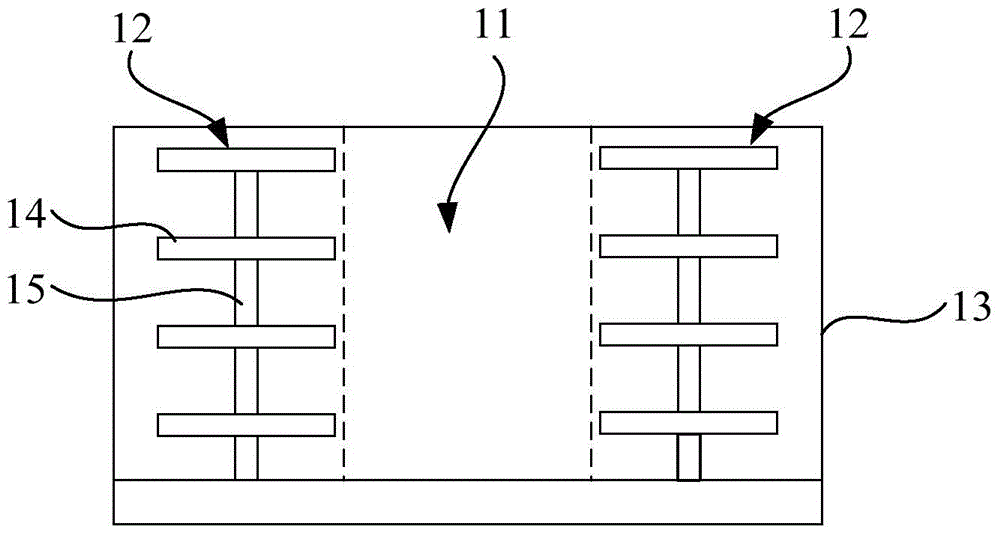
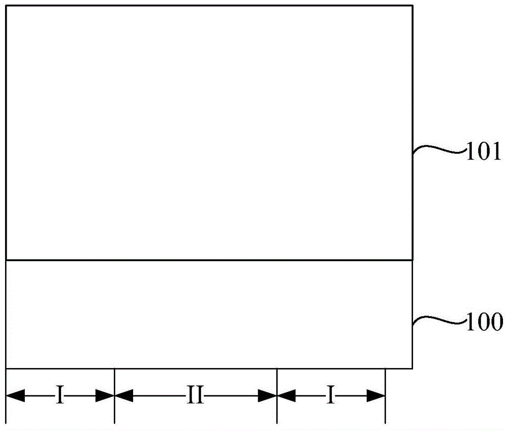
[0041] refer to image 3 A wafer 100 is provided, and the wafer 100 is divided into a plurality of chip regions I and a dicing line II located between two adjacent chip regions I. Cutting lane II is the subsequent wafer cutting position.

[0042] A device structure located in the wafer is formed in the chip area I, and the device structure is a functional device that can realize a specific function. However, no functional device is formed in the wafer at the position of dicing line II.

[0043] In a specific embodiment, the wafer 100 may be a silicon wafer, or may be a germanium, silicon germanium, gallium arsenide or silicon-on-insulator wafer. Those skilled in the art can select wafers according to needs, so the type of wafers should ...


PUM


Abstract

A semiconductor device and its forming method, and a method for improving wafer cutting yield, wherein the forming method of the semiconductor device includes: providing a wafer, the wafer is divided into a plurality of chip areas, and cutting between two adjacent chip areas The interlayer dielectric layer is formed on the wafer; the multilayer interconnection metal layer and the multilayer plug layer corresponding to the chip area are formed in the interlayer dielectric layer, and the plug layer is passed between two adjacent interconnection metal layers Electrical connection; multiple layers of dummy plug layers corresponding to dicing lines are formed in the interlayer dielectric layer, and each dummy plug layer includes a plurality of dummy plugs. When cutting a semiconductor device along the scribe line, the stress generated at the scribe line position mainly acts on the dummy plug, and the interlayer dielectric layer part of the chip area and the plug layer therein will not be subjected to stress or only a small stress, preventing the chip The part of the interlayer dielectric layer in the region and the plug layer in it are broken, so as to ensure that the interconnection performance of the interconnection metal layer and the plug layer in the chip region is good. This significantly improves wafer dicing yield.

Description

technical field [0001] The invention relates to the technical field of semiconductors, in particular to a semiconductor device, a method for forming the same, and a method for improving the wafer cutting yield. Background technique [0002] In the semiconductor manufacturing process, the wafer formed with integrated circuits is usually cut into individual chips, and then these chips are made into semiconductor packaging structures with different functions. [0003] refer to figure 1 , figure 1 It is a top view of the wafer, the wafer is composed of a plurality of chips 10 , and two adjacent chips 10 are separated by scribe lines 11 . For each chip 10, a device structure, an interconnection structure, and pads are formed on a substrate through processes such as deposition, lithography, etching, doping, and heat treatment. Afterwards, the wafer is diced into a plurality of independent chips 10 along the dicing lines 11 , so there are no functional elements at the positions ...

Claims


Application Information

Patent Timeline
Patent Type & Authority Patents(China)
IPC IPC(8): H01L21/768H01L23/522H01L21/78
Inventor 马振勇刘文晓戴海波李日鑫
Owner SEMICON MFG INT (SHANGHAI) CORP
Why Eureka
Try Eureka