Chip formation method and method for increasing yield of packaged finished product

A chip packaging and chip technology, which is applied in the field of chip formation methods and improving the yield rate of chip packaging products, can solve problems such as chip performance not meeting the design requirements, chip functions not working normally, chip failure, etc., to achieve good interconnection performance , enhance the mechanical strength, avoid the effect of interference

Active Publication Date: 2015-06-10
SPREADTRUM COMM (SHANGHAI) CO LTD
View PDF6 Cites 0 Cited by
  • Summary
  • Abstract
  • Description
  • Claims
  • Application Information

AI Technical Summary

Problems solved by technology

In this way, the interconnection between two adjacent interconnected metal layers will be disconnected (Open), causing the chip to fail, for example, some functions of the chip cannot work normally or the performance of the chip cannot meet the design requirements, resulting in a high yield rate. reduce

Method used


Image

  • Chip formation method and method for increasing yield of packaged finished product
  • Chip formation method and method for increasing yield of packaged finished product
  • Chip formation method and method for increasing yield of packaged finished product

Examples


Embodiment Construction

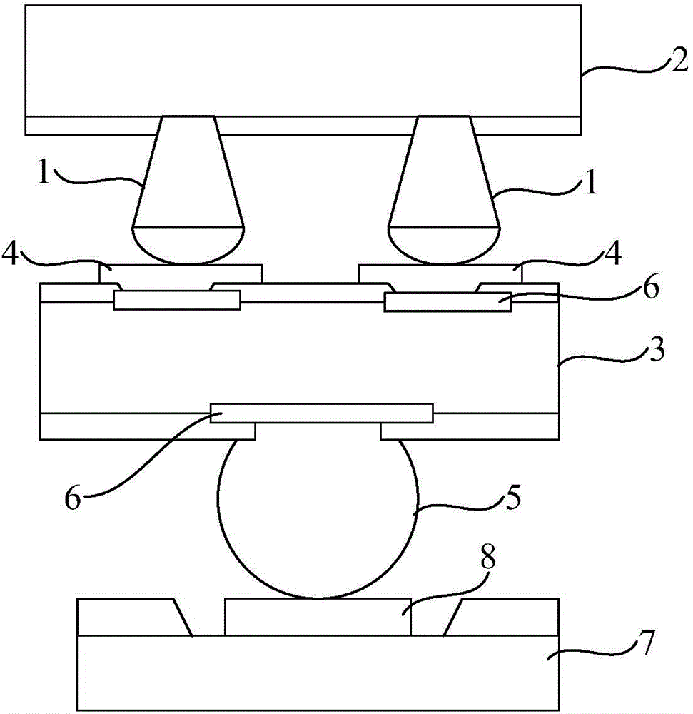
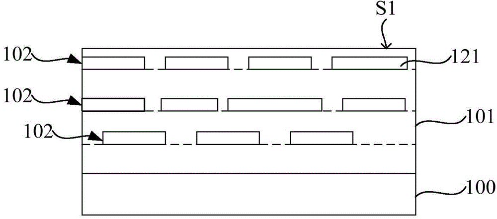
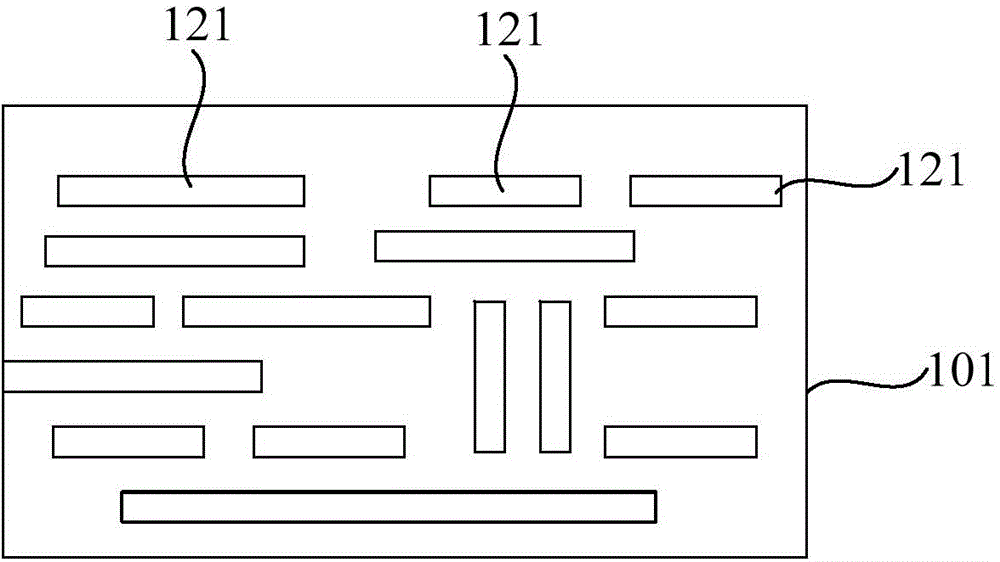
[0031] In view of the problems existing in the prior art, through statistical analysis, it is found that: in the direction perpendicular to the front of the chip, among the two interconnected metal layers on both sides of the interlayer dielectric material layer where the fracture occurs, one or two interconnected layers The metal density of the metal layer is relatively small, about less than 0.3. The metal density refers to the ratio of the projected surface area of ​​a layer of interconnection metal layer directly below the copper pillar bump on the front surface of the chip to the surface area occupied by the copper pillar bump on the front surface of the chip. When the metal density of a layer of interconnect metal layer under the copper pillar bump is less than 0.3, the mechanical strength of the interlayer dielectric material layer on both sides of the interconnect metal layer perpendicular to the direction of the front of the chip is insufficient. , It is easy to cause...


PUM


Abstract

Disclosed are a chip formation method and a method for increasing yield of a packaged finished product. The chip formation method includes providing a chip graph comprising a plurality of interconnection metal layer graphs, wherein when the metal density of one of the interconnection metal layer graphs is smaller than 0.3, a filling metal wire graph is formed in a gap of the interconnection metal layer graph to enable the metal density of the interconnection metal layer graph and the filling metal wire graph to be larger than or equal to 0.3; forming a chip according to the chip graph. In the phase of chip graph design, the metal density of the interconnection metal layer graphs is larger than or equal to 0.3, and interconnection metal layers and filling metal wire layers are produced according to the interconnection metal layer graphs and the filling metal wire graphs; during packaging, interlayer dielectric material layer portions at positions, between every two adjacent interconnection metal layers, below raised points of a soldering flux can bear high mechanical stress, the risk of breakage of the interlayer dielectric material layer portions and plugging layers is avoided or even eliminated, and the yield of the packaged finished product meets mass production requirements.

Description

technical field [0001] The invention relates to the technical field of semiconductors, in particular to a method for forming a chip and a method for improving the yield rate of chip packaging products. Background technique [0002] In the semiconductor chip packaging process, solder bumps are formed on the front of the chip, and then the chip is flipped over and connected to the packaging substrate, electrically and mechanically connected to the circuit. This packaging method is called flip chip packaging (flip chip) method . [0003] refer to figure 1 , the existing high-density I / O chips of 40nm / 28nm process of semiconductor technology generally adopt the flip-chip packaging method based on copper pillar bump (Copper Pillar Bump) 1 . A plurality of copper pillar bumps 1 distributed on the front surface of the chip 2 are soldered to bump pads (Bump Pads) 4 on the front surface of the substrate 3 respectively. Next, solder balls (Solder Ball) 5 are formed on the back surf...

Claims


Application Information

Patent Timeline
Patent Type & Authority Applications(China)
IPC IPC(8): H01L21/768
CPCH01L21/76886H01L2221/1068
Inventor 郭叙海
Owner SPREADTRUM COMM (SHANGHAI) CO LTD
Why Eureka
Try Eureka