LED light emitting material

A technology of light-emitting material and hole injection layer, applied in electrical components, circuits, semiconductor devices, etc., can solve the problem of low light-emitting efficiency of LED light-emitting materials, and achieve the effect of improving light-emitting efficiency, avoiding interface defects and high light-emitting efficiency

Inactive Publication Date: 2015-07-01
CHANGCHUN INST OF OPTICS FINE MECHANICS & PHYSICS CHINESE ACAD OF SCI
View PDF4 Cites 3 Cited by
  • Summary
  • Abstract
  • Description
  • Claims
  • Application Information

AI Technical Summary

Problems solved by technology

[0003] The purpose of the present invention is to solve the technical problem of low luminous efficiency of LED luminescent materials in the prior art, and provide a kind of LED luminescent material

Method used


Image

  • LED light emitting material
  • LED light emitting material

Examples


Embodiment 1

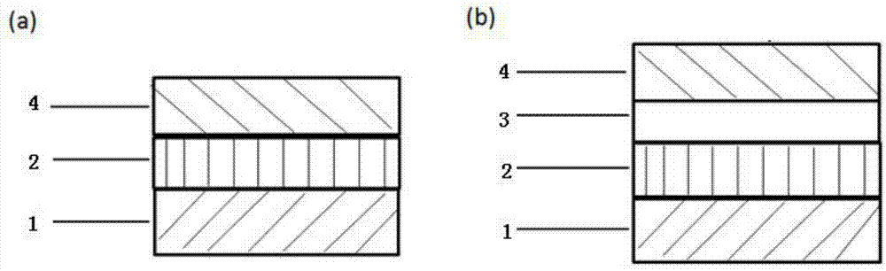
[0029] LED luminescent materials, from bottom to top: 600nm thick p-GaN, 150nm thick p-ZnO, 400nm thick n-ZnO.

[0030] The preparation method of the above-mentioned LED luminescent material:

[0031] Step 1. On the sapphire substrate, grow a film with a thickness of 600nm and a hole concentration of 10 17 cm -3 p-GaN;

[0032] Step 3, grow a layer on p-GaN with a thickness of 150nm and a hole concentration of 10 16 cm -3 p-ZnO;

[0033] Step 4, growing a layer of n-ZnO with a film thickness of 400 nm on the p-ZnO to obtain an LED luminescent material.

[0034] Using the vacuum thermal evaporation process to vapor-deposit metal nickel-gold film (Ni / Au) and metal indium (In) on p-GaN and n-ZnO respectively as contact electrodes, the LED luminescent material is deviceized, and the LED luminescent material is deviceized. When the injection current is 60mA, the measured output power of the deviceized LED is 20μw.

Embodiment 2

[0036] LED luminescent materials, from bottom to top: 400nm thick n-ZnO, 150nm thick p-ZnO, 600nm thick p-GaN.

[0037] The preparation method of the above-mentioned LED luminescent material:

[0038] Step 1, growing a layer of n-ZnO with a film thickness of 400nm on the sapphire substrate;

[0039] Step 2, grow a film on n-ZnO with a thickness of 150nm and a hole concentration of 10 16 cm -3 p-ZnO;

[0040]Step 3, grow a film thickness of 600nm on p-ZnO, the hole concentration is 10 17 cm -3 p-GaN to obtain LED light-emitting materials.

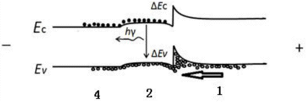
[0041] Using the vacuum thermal evaporation process to vapor-deposit metal nickel-gold film (Ni / Au) and metal indium (In) on p-GaN and n-ZnO respectively as contact electrodes, the LED light-emitting materials are deviceized. When the injection current is 60mA, It is measured that the output power of the deviceized LED is 2 μw. It can be seen from Comparative Example 1 and Examples 1-2 that the output power of the LED luminescent mate...

Embodiment 3

[0043] LED luminescent materials, from bottom to top: 600nm thick p-diamond, 150nm thick p-ZnO, 400nm thick n-ZnO.

[0044] The preparation method of the above-mentioned LED luminescent material:

[0045] Step 1. On the sapphire substrate, grow a film with a thickness of 600nm and a hole concentration of 10 18 cm -3 p-diamond;

[0046] Step 2: Grow a layer on p-diamond with a thickness of 150nm and a hole concentration of 10 16 cm -3 p-ZnO;

[0047] Step 3: growing a layer of n-ZnO with a film thickness of 400 nm on the p-ZnO to obtain an LED luminescent material.

[0048] The vacuum thermal evaporation process is used to vapor-deposit metal nickel-gold film (Ni / Au) and metal indium (In) on p-diamond and n-ZnO respectively as contact electrodes, and LED light-emitting materials are deviceized.


PUM


Abstract

The invention discloses an LED light emitting material, belongs to the technical field of semiconductor photoelectron materials and devices and solves the technical problem that LED light emitting materials are low in light emitting efficiency in the prior art. The LED light emitting material comprises a P(I)N junction and a hole injection layer, the hole injection layer closely contacts with a p-type layer of the P(I)N junction, carrier concentration of the hole injection layer is larger than hole concentration in the p-type layer, and thickness of the hole injection layer is 50nm-3micron. The LED light emitting material is of a homogeneous structure, so that interface defect caused by heterostructure is avoided; hole concentration of the p-type layer is increased by adopting the hole injection layer, so that the LED light emitting material has high light emitting efficiency.

Description

technical field [0001] The invention belongs to the technical field of semiconductor optoelectronic materials and devices, and in particular relates to an LED luminescent material. Background technique [0002] Light-emitting diodes, referred to as LEDs, have the advantages of low operating voltage, small operating current, good shock resistance and shock resistance, high reliability, long life, and the intensity of light can be easily modulated by modulating the intensity of the current. However, some semiconductor light-emitting materials, such as ZnO, GaN, AlGaN, MgZnO, SiC, diamond, etc., have very low luminous efficiency and cannot even be observed. Therefore, it is necessary to enhance the luminous efficiency of these materials before application. LEDs emit light through the recombination radiation of electrons and holes in their structure, so the luminous intensity of LEDs usually depends on the number of electrons and holes in the light-emitting layer. For some semi...

Claims


Application Information

Patent Timeline
Patent Type & Authority Applications(China)
IPC IPC(8): H01L33/02
CPCH01L33/14H01L33/025
Inventor 单崇新刘凯凯王双鹏卢英杰申德振
Owner CHANGCHUN INST OF OPTICS FINE MECHANICS & PHYSICS CHINESE ACAD OF SCI
Why Eureka
Try Eureka