Flip LED chip packaging method and flip LED chip using packaging method

A technology of LED chip and packaging method, which is applied in the direction of electrical components, circuits, semiconductor devices, etc., and can solve the problems of low production efficiency and large equipment investment

Active Publication Date: 2015-07-01
LEEDARSON IOT TECH INC
View PDF4 Cites 4 Cited by
  • Summary
  • Abstract
  • Description
  • Claims
  • Application Information

AI Technical Summary

Problems solved by technology

This process has the disadvantages of requiring a large am

Method used


Image

  • Flip LED chip packaging method and flip LED chip using packaging method
  • Flip LED chip packaging method and flip LED chip using packaging method
  • Flip LED chip packaging method and flip LED chip using packaging method

Examples


Example Embodiment

[0013] The present invention will be further described in detail below in conjunction with the drawings and specific embodiments.

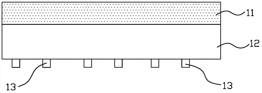
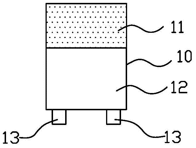
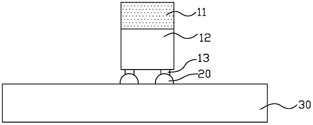
[0014] Figure 1 to Figure 4 It is a schematic diagram of the relevant structure of the packaging method of the flip-chip LED chip of the present invention. Please refer to Figure 4 The flip-chip LED chip 10 is disposed on the substrate 30 and includes a packaging layer that encapsulates the LED chip 10 on the substrate 30.

[0015] Please refer to Figure 4 The encapsulation layer is formed by a thin film 11 disposed on the epitaxial wafer 12 of the flip-chip LED chip 10 when the LED chip 10 is welded to the substrate 30 and melted to cover the LED chip 10 and then solidified. The film 11 includes a first layer at the bottom and a melting layer (not shown) at the first layer. The melting point of the first layer is higher than the maximum temperature of reflow soldering. The first layer is directly connected to the epitaxial wafer 12 . The tempera...


PUM


Abstract

The invention discloses a flip LED chip packaging method. The method comprises steps: an epitaxial slice of the flip LED chip is firstly made; a thin film is fixed at the top part of the epitaxial slice; electrodes are made on the epitaxial slice so as to form a flip LED chip; a solder paste is arranged on a substrate to enable two electrodes of the LED chip to be contacted with the solder paste respectively, reflow soldering is then carried out on the substrate and the LED chip on the substrate, and thus the electrodes of the LED chip are soldered on the substrate; and the thin film is heated and melted during the reflow soldering process and coats the LED chip, and then the thin film is cooled and cured to form a packaging layer. In addition, the invention also provides a flip LED chip using the packaging method. The flip LED chip packaging method and the flip LED chip using the packaging method have the advantages of a simple production process.

Description

technical field [0001] The invention relates to the technical field of LED packaging, in particular to a packaging method for a flip-chip LED chip and a flip-chip LED chip using the packaging method. Background technique [0002] There are many packaging methods for LEDs. At present, a common packaging method in the industry is to complete the process by welding the chip first and then coating phosphor powder. For example, the patent application No. 201110431854.1 published on June 26, 2013 discloses a white LED packaging process. The packaging process of the white light LED includes the following steps: a. providing a packaging bracket, a light-transmitting cover and a blue LED flip-chip; b. solidifying the blue LED flip-chip on the packaging bracket; c. welding wires , the positive and negative electrodes of the blue LED flip chip are electrically connected to the first electrode and the second electrode on the packaging bracket respectively; d, dispensing glue, filling t...

Claims


Application Information

Patent Timeline
IPC IPC(8): H01L33/62
CPCH01L33/48H01L33/52H01L33/62H01L2933/0033H01L2933/005
Inventor 马志超郭伟杰李甫文
Owner LEEDARSON IOT TECH INC
Why Eureka
Try Eureka