Implant-induced damage control in ion implantation

An ion implantation system and ion beam technology, which are used in ion implantation plating, semiconductor devices, semiconductor/solid-state device testing/measurement, etc., can solve problems such as damage to the lattice structure of workpieces

Active Publication Date: 2015-07-01
AXCELIS TECHNOLOGIES
View PDF3 Cites 4 Cited by
  • Summary
  • Abstract
  • Description
  • Claims
  • Application Information

AI Technical Summary

Problems solved by technology

However, damage to the workpiece lattice structure due to high dose and / or high energy implants in a single workpiece framework has been problematic

Method used


Image

  • Implant-induced damage control in ion implantation
  • Implant-induced damage control in ion implantation
  • Implant-induced damage control in ion implantation

Examples


Embodiment Construction

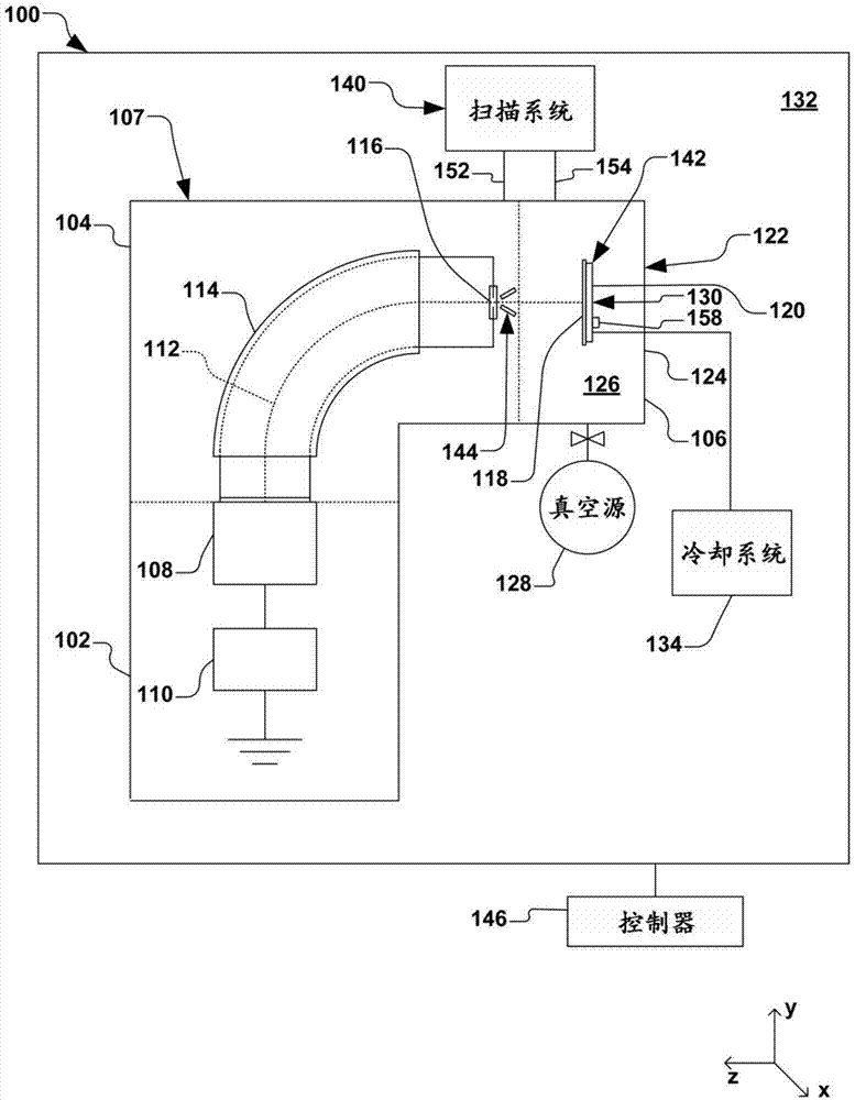
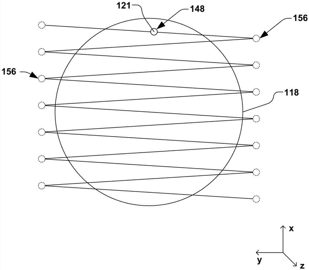
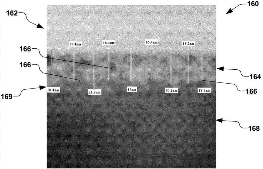
[0019] The present invention is generally directed to a device, system and method for controlling the accumulation of local damage on a semiconductor workpiece, and at the same time optimizing the workpiece throughput in a single workpiece ion implantation framework. Accordingly, the present invention will now be explained with reference to the drawings, in which the same reference numerals throughout the text may be used to refer to the same elements. It should be understood that the description of these aspects is for illustrative purposes only and shall not be interpreted as limiting purposes. For explanatory purposes, several specific details are set forth below in order to fully understand the present invention. However, it will be obvious to those skilled in the art that the present invention can be implemented without these specific details. In addition, the scope of the present invention should not be limited by the embodiments or examples described below with referenc...


PUM


Abstract

An ion implantation system is provided having an ion implantation apparatus configured to provide a spot ion beam having a beam density to a workpiece, wherein the workpiece has a crystalline structure associated therewith. A scanning system iteratively scans one or more of the spot ion beam and workpiece with respect to one another along one or more axes. A controller is also provided and configured to establish a predetermined localized temperature of the workpiece as a predetermined location on the workpiece is exposed to the spot ion beam. A predetermined localized disorder of the crystalline structure of the workpiece is thereby achieved at the predetermined location, wherein the controller is configured to control one or more of the beam density of the spot ion beam and a duty cycle associated with the scanning system to establish the localized temperature of the workpiece at the predetermined location on the workpiece.

Description

Technical field [0001] The present invention relates generally to an ion implantation system, and more specifically to a control of the scanning frequency and duty cycle of a scanning point ion beam, so as to control the rate of accumulation of damage induced by implantation in a workpiece. Background technique [0002] With the emphasis on wireless and portable technologies, the continuous and rapid development of electronic devices has brought new challenges to semiconductor manufacturing. The development of device technology requires smaller transistors with better performance. Improving device performance and reducing harmful leakage current in the device have become the focus of attention. The semiconductor manufacturing process that contributes to the harmful leakage current in the output device is the ion implantation process. [0003] Based on many factors, ion implantation can cause damage to the lattice structure of semiconductor workpieces (such as silicon), including ...

Claims


Application Information

Patent Timeline
Patent Type & Authority Applications(China)
IPC IPC(8): H01J37/304H01J37/317
CPCH01J37/3171H01J2237/31703H01J2237/30472H01L2924/0002H01J2237/30455H01L22/26C23C14/48H01J37/304H01L2924/00
Inventor 罗纳德·里斯谢尔盖·孔德拉坚科舒·佐藤安德鲁·雷
Owner AXCELIS TECHNOLOGIES
Why Eureka
Try Eureka