A source-drain electrode of a thin film transistor and its preparation method, a thin film transistor and its preparation method

A technology of thin-film transistors and source-drain electrodes, applied in the field of preparation of thin-film transistors, can solve problems such as easy oxidation of copper, high contact resistance, and peeling, and achieve the effects of reduced electrode peeling rate, improved transmission performance, and improved bonding strength

Active Publication Date: 2019-01-29
SOUTH CHINA UNIV OF TECH
View PDF3 Cites 0 Cited by
  • Summary
  • Abstract
  • Description
  • Claims
  • Application Information

AI Technical Summary

Problems solved by technology

Silver is prone to aggregation of silver particles during deposition, which seriously affects electron transport. In addition, the cost of silver is very expensive, which limits the use of silver electrodes.
[0006] Copper is ideal in terms of resistivity, stability and cost, but copper has the following problems: 1) copper is easily oxidized, and the resistivity of copper oxide is relatively high; 2) copper electrodes are deposited on metal oxides. After the source layer is on, copper atoms will diffuse to the oxide, and acceptor-like defects will be generated in the active layer, which will degrade the electrical properties of the active layer; 3) The contact resistance between copper (including silver) and metal oxides is high, It shows that the energy level does not match; 4) The copper electrode itself has tensile stress (stress > 0), and it will warp and peel off after being deposited on the active layer

Method used


Image

  • A source-drain electrode of a thin film transistor and its preparation method, a thin film transistor and its preparation method
  • A source-drain electrode of a thin film transistor and its preparation method, a thin film transistor and its preparation method
  • A source-drain electrode of a thin film transistor and its preparation method, a thin film transistor and its preparation method

Examples


Embodiment 1

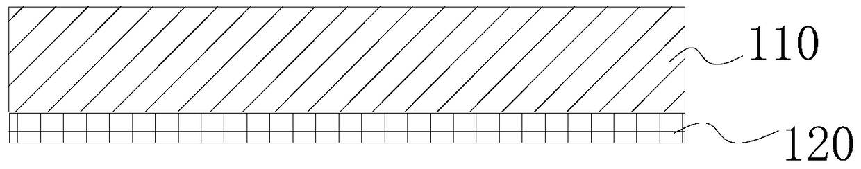
[0045] The source and drain electrodes of the thin film transistor of this embodiment are as figure 1 As shown, it is composed of a molybdenum layer 120 and a copper layer 110 stacked in sequence, the copper layer 110 is located above the molybdenum layer 120, and the molybdenum layer 120 is disposed above the active layer of the thin film transistor.

[0046] Wherein, the thickness of the molybdenum layer is set to be 20-40 nm. The thickness of the copper layer is set to 150-250 nm. In this embodiment, the thickness of the copper layer is preferably set to 200 nm, and the thickness of the molybdenum layer is set to 30 nm.

[0047] The preparation method of the source and drain electrodes of the thin film transistor of this embodiment is as follows:

[0048] (1) Under the Ar gas environment of 10sccm, the air pressure is 1mTorr, with 50 watts of power, the molybdenum film is prepared as the molybdenum layer in the sputtering of the active layer of the thin film transistor;

...

Embodiment 2

[0059] Such as Figure 4 As shown, the thin film transistor of this embodiment includes a substrate 200, a bottom gate 300, a gate insulating layer 400, an active layer 500, and a source-drain electrode 100 from bottom to top; layers and copper layers.

[0060] The preparation process of the thin film transistor of this embodiment is as follows:

[0061] a. First, a 300nm aluminum alloy film is deposited on the glass substrate by DC sputtering and wet etching as the bottom gate;

[0062] b. Then prepare a layer of 200nm Al on the bottom gate by chemical anodic oxidation 2 o 3 gate insulating layer;

[0063] c. A 50nm a-IGZO thin film is used as the active layer by radio frequency magnetron sputtering at room temperature, and the a-IGZO thin film is patterned by wet etching, and then annealed in an air atmosphere at 300 ° C for 30 min;

[0064] d. Under the Ar gas environment of 10sccm, the air pressure is 1mTorr, sputtering a molybdenum 30nm film with a power of 50 watts ...

Embodiment 3

[0067] The preparation process of the thin film transistor of this embodiment is as follows:

[0068] a. First, a 300nm aluminum alloy film is deposited on the glass substrate by DC sputtering and wet etching as the bottom gate;

[0069] b. Then prepare a layer of 200nm Al on the bottom gate by chemical anodic oxidation 2 o 3 gate insulating layer;

[0070] c. A 50nm a-IGZO thin film is used as the active layer by radio frequency magnetron sputtering at room temperature, and the a-IGZO thin film is patterned by wet etching, and then annealed in an air atmosphere at 300 ° C for 30 min;

[0071] d. Under the Ar gas environment of 25sccm, the air pressure is 7mTorr, sputtering molybdenum 30nm thin film with 200 watts of power as the molybdenum layer, then under the Ar gas environment of 10sccm, the air pressure is 7mTorr, sputtering 100nm copper thin film with 100 watts of power as the molybdenum layer Copper layer; then, the prepared molybdenum layer and copper layer are patt...


PUM

PropertyMeasurementUnit
thicknessaaaaaaaaaa
thicknessaaaaaaaaaa
electron work functionaaaaaaaaaa

Abstract

The invention discloses a source-drain electrode of a thin film transistor. The source-drain electrode is composed of a molybdenum layer and a copper layer in a sequential overlaying mode, and the copper layer is arranged on the molybdenum layer. The molybdenum layer is arranged on an active layer of the thin film transistor; the growth direction of crystal lattices of the molybdenum layer and the growth direction of crystal lattices of the copper layer are perpendicular to each other; the thickness of the molybdenum layer is 20 nm-40 nm; the thickness of the copper layer is 150 nm-250 nm. The invention further discloses a manufacturing method of the source-drain electrode, the thin film transistor comprising the source-drain electrode and a manufacturing method of the thin film transistor. The defects that in the prior art, copper electrodes are prone to being oxidized, and copper atoms diffuse toward oxide after the copper electrodes deposit on the active layer of the metal oxide are overcome, the source-drain electrode has the advantage of high conductivity, stress balance between two layers of electrodes can be achieved, the disbanding ratio of the electrodes is lowered, and the bonding strength is improved.

Description

technical field [0001] The invention relates to the field of preparation of thin film transistors, in particular to a source and drain electrode of a thin film transistor and a preparation method, the thin film transistor and a preparation method. Background technique [0002] A thin film transistor (Thin Film Transistor, TFT for short) is a semiconductor device with a wide range of uses, and is mainly used in displays to drive liquid crystal alignment changes, or to drive OLED pixels to emit light. The structure of the thin film transistor at least includes a gate, a gate insulating layer, an active layer, and source and drain electrodes. [0003] With the popularity of large-size, high-resolution, high-refresh rate displays, TFT must have excellent mobility and conductivity in order to shorten signal delay, reduce energy consumption, and improve display quality. [0004] The mobility is mainly determined by the active layer material of the TFT. Currently popular active l...

Claims


Application Information

Patent Timeline
Patent Type & Authority Patents(China)
IPC IPC(8): H01L29/786H01L29/45H01L21/44
CPCH01L29/41733H01L29/45H01L29/66742H01L29/786
Inventor 宁洪龙胡诗犇朱峰兰林锋彭俊彪王磊
Owner SOUTH CHINA UNIV OF TECH
Why Eureka
Try Eureka