Plasmonic all-optical logic device based on aperture resonant coupling effect

A plasmonic and resonant coupling technology, applied in logic circuits using optoelectronic devices, logic circuits using specific components, logic circuits, etc., can solve problems such as influence, achieve long transmission distance, low radiation loss, reduce incident The effect of optical power

Active Publication Date: 2017-10-03
INST OF SEMICONDUCTORS - CHINESE ACAD OF SCI
View PDF2 Cites 2 Cited by
  • Summary
  • Abstract
  • Description
  • Claims
  • Application Information

AI Technical Summary

Problems solved by technology

[0005] The present invention designs a plasmonic all-optical logic device based on the resonant coupling effect of the aperture, and it is necessary to solve the problem of the influence of the displacement of the coupling aperture along the lateral and vertical directions on the parallel shunting of the induced current on the side wall of the air hole, and the outside of the cube particles. Corresponding relationship between the intensity of resonance output of different ports and the wavelength caused by the interference of plasmon waves caused by the wall magneto-induced current

Method used


Image

  • Plasmonic all-optical logic device based on aperture resonant coupling effect
  • Plasmonic all-optical logic device based on aperture resonant coupling effect
  • Plasmonic all-optical logic device based on aperture resonant coupling effect

Examples


Embodiment 1

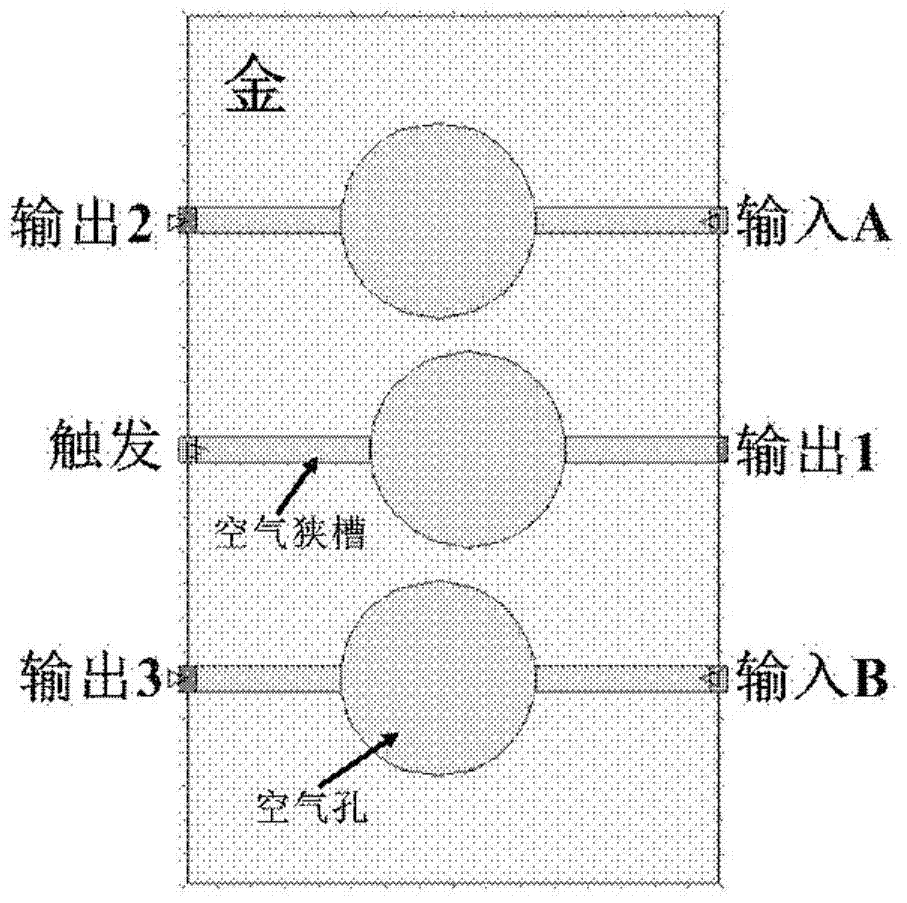
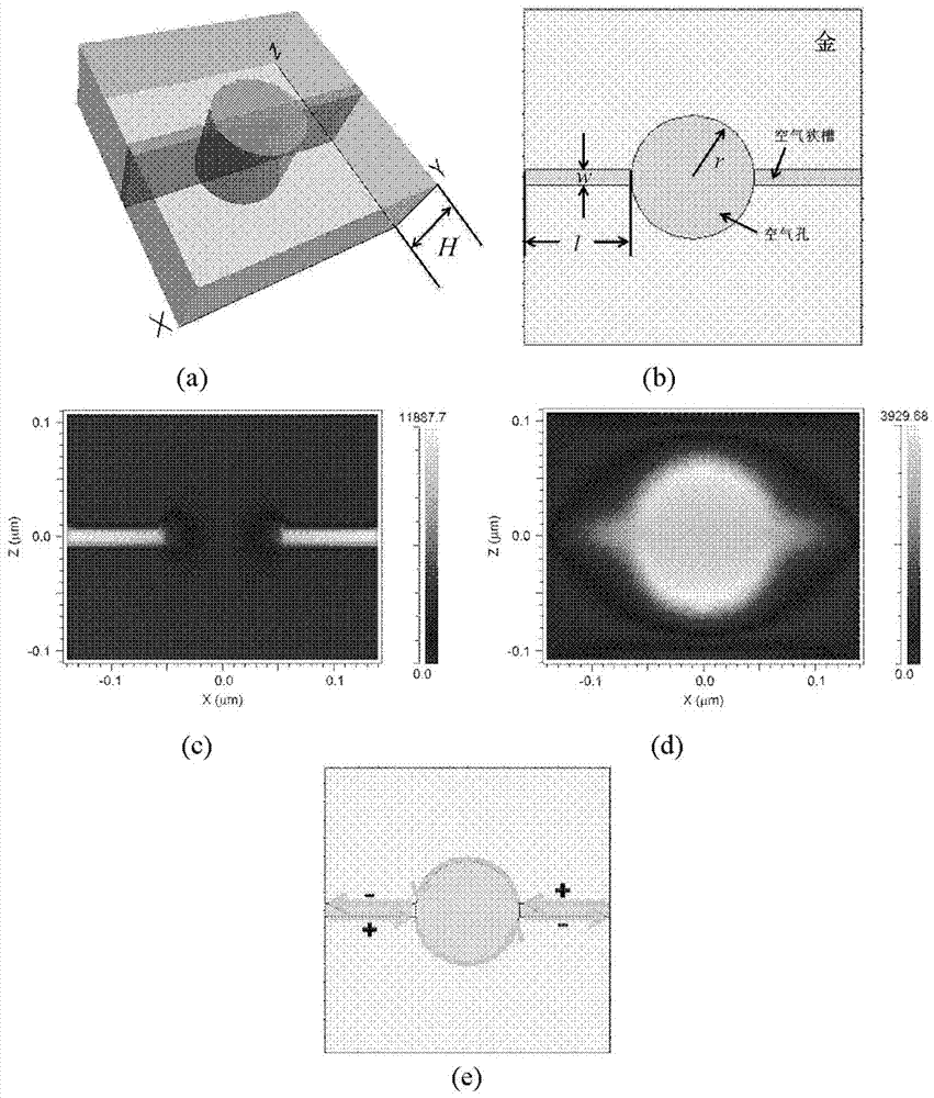
[0037] figure 2 (a)(b) shows a single opening structure, which is composed of an air slot and an air hole etched on a cube-shaped gold particle, and the slot passes through the center of the air hole. Air hole radius r=58nm, air slot length l=100nm on both sides of the air hole, groove width w=15nm, cube thickness H=105nm. figure 2 (c) is the distribution diagram of the electric field intensity, figure 2 (d) is the magnetic field intensity distribution diagram. Obviously, the electric field is mainly localized in the air slots, while the magnetic field is mainly localized in the air holes. Here the dimensions of the air slot mainly allow the existence of the magnetoplasmonic fundamental mode. It can be seen from the color scale diagram that the maximum value of the electric field intensity in the structure is obviously greater than that of the magnetic field, but the intensity of the magnetic field is higher than that of the electric field at a place slightly away from t...


PUM


Abstract

The invention relates to a plasmonic all-optical logic device based on the resonant coupling effect of an aperture, which uses three aperture resonators to adjust in the horizontal and vertical dimensions to change the coupling strength to enrich the output state of each port, which has a small size , low power consumption, and belongs to the field of optoelectronic integration technology.

Description

technical field [0001] The invention relates to the technical field of optoelectronic integration, in particular to a plasmonic all-optical logic device based on an aperture resonator. Background technique [0002] Today's state-of-the-art microprocessors are based primarily on ultra-fast nanoscale transistors, with dimensions on the order of 50 nanometers. Routine production of fast transistors is not a problem these days, the main problem is how to get the digital information to the other end of the microprocessor, which is about a few centimeters away. As the number of integrated transistors in a circuit increases exponentially, it is no longer sufficient to connect them with copper wires. The aggravation of information delay in the connection has also become a bottleneck that hinders the further improvement of the speed of digital circuits. With the acceleration of microprocessors, its annual growth rate has obviously slowed down in the past one or two years. [0003]...

Claims


Application Information

Patent Timeline
Patent Type & Authority Patents(China)
IPC IPC(8): G02B6/122G02F3/00
Inventor 郑婉华王宇飞祁帆马庆艳王少华
Owner INST OF SEMICONDUCTORS - CHINESE ACAD OF SCI
Why Eureka
Try Eureka