double-sided photolithography

A double-sided photolithography and photolithography technology, which is applied in the direction of optics, optomechanical equipment, and photolithography on the pattern surface, etc., can solve problems such as rotation deviation, inaccurate mask alignment, and the impact of alignment accuracy

Active Publication Date: 2017-08-08
CSMC TECH FAB2 CO LTD
View PDF6 Cites 0 Cited by
  • Summary
  • Abstract
  • Description
  • Claims
  • Application Information

AI Technical Summary

Problems solved by technology

However, inaccurate alignment is common in manual placement of masks, including center deviation, that is, the center of the exposure pattern will deviate from the center of the wafer, and the maximum deviation will reach more than ten millimeters; it also includes rotation deviation, that is, the exposure pattern is relative to the wafer. The flat side of the circle will rotate, up to tens of degrees
Although skilled workers can overcome this problem to a large extent, alignment accuracy is still affected by operating proficiency

Method used


Image

  • double-sided photolithography
  • double-sided photolithography
  • double-sided photolithography

Examples


Embodiment Construction

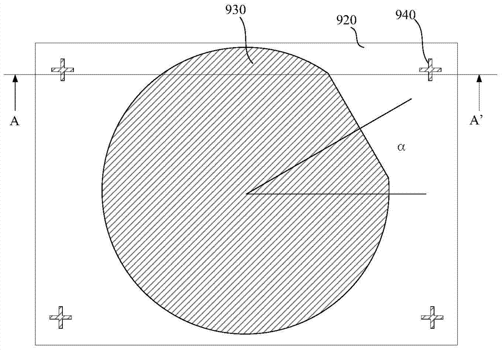
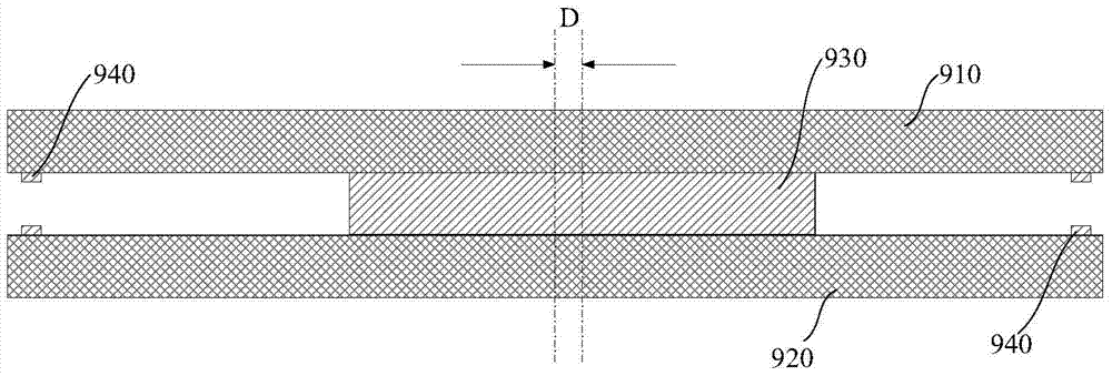
[0015] figure 1 It is a plan view of the positional relationship between the lithography plate and the substrate in a traditional double-sided lithography process, figure 2 for figure 1 Sectional view along the A-A' section line. Most of the double-sided lithography adopts proximity or contact exposure, so the ratio of the pattern on the lithography plate to the pattern finally imaged on the substrate is 1:1. reference figure 2 The principle of traditional double-sided lithography is to sandwich the substrate 930 between the upper plate 910 and the lower plate 920, and then use a clamp to send it to the exposure machine for exposure, so that the pattern can be directly formed on the substrate . Alignment marks 940 are used between the upper plate 910 and the lower plate 920 for alignment. However, although the upper plate 910 and the lower plate 920 can be aligned by the alignment marks 940, the substrate 930 and the upper plate 910 or the lower plate 920 are aligned. Howeve...


PUM


Abstract

The invention discloses a double-sided photolithography method, comprising the following steps: making a first alignment mark (101) on one side or both sides of a substrate (100) to be photoetched; using the first alignment mark (101) ) to align the photolithography plate and the substrate (100) used for the first photolithography, and make graphics and second alignment marks (103) on the substrate (100); using the second alignment marks ( 103) Aligning the photolithography plate and the substrate (100) used for subsequent photolithography, and making subsequent patterns on the substrate (100); the accuracy of the first alignment mark (101) is higher than that of the second Accuracy of registration marks (103). The above method can prevent the pattern from shifting on the substrate.

Description

Technical field [0001] The invention relates to semiconductor manufacturing, in particular to a zero-time exposure method of a double-sided photoetching machine. Background technique [0002] In the semiconductor process, there are some cases where a double-sided processing process is required, for example, when patterns need to be made on both the front and back sides of the silicon wafer, or the size of the chip is larger than 2mm. The double-sided processing technology requires special equipment, a double-sided lithography machine. [0003] The double-sided lithography machine uses proximity or contact exposure, that is, the optical system projects the pattern onto the silicon wafer at a ratio of 1:1. Therefore, the mask used is the same size as the silicon wafer, and the size and position of the pattern on the mask must also be consistent with the actual situation. In this way, the traditional double-sided photolithography process basically uses manual methods to place and al...

Claims


Application Information

Patent Timeline
Patent Type & Authority Patents(China)
IPC IPC(8): G03F9/00G03F7/00
Inventor 荆二荣
Owner CSMC TECH FAB2 CO LTD
Why Eureka
Try Eureka