Clock signal generation circuit, grid driving circuit, display panel and display device

A gate drive circuit and clock signal technology, which is applied in the field of gate drive circuit, clock signal generation circuit, display panel and display device, can solve problems such as distortion, heavy load, and clock signal distortion, and achieve the target clock signal accuracy, Avoid insufficient charging and ensure the effect of display effect

Inactive Publication Date: 2015-07-29
HEFEI BOE OPTOELECTRONICS TECH +1
View PDF5 Cites 14 Cited by
  • Summary
  • Abstract
  • Description
  • Claims
  • Application Information

AI Technical Summary

Problems solved by technology

[0003] In the existing TFT LCD, the clock signal is connected to multiple rows of pixels, and its load is relatively large. This will cause the increase in the number of pixel rows scanned by the gate drive circuit when each frame is displayed, due to the resistance in the signal transmission line (there is resistance in the signal line) and capacitance (the shift register is equivalent to capacitance), the clock signal will gradually attenuate and be distorted; especially in TFT LCD with higher resolution, due to its large number of rows, in When scanning to several rows at the far end, the distortion of the clock signal may even lead to insufficient charging, which cannot drive the pixels of these rows to turn on
For example, if figure 1 As shown, when the gate drive circuit scans the nth row of pixels, the clock signal has been obviously distorted. The thin film transistors are turned on, so that the display of the row of pixels cannot

Method used


Image

  • Clock signal generation circuit, grid driving circuit, display panel and display device
  • Clock signal generation circuit, grid driving circuit, display panel and display device
  • Clock signal generation circuit, grid driving circuit, display panel and display device

Examples


Embodiment Construction

[0029] Specific embodiments of the present invention will be described in detail below in conjunction with the accompanying drawings. It should be understood that the specific embodiments described here are only used to illustrate and explain the present invention, and are not intended to limit the present invention.

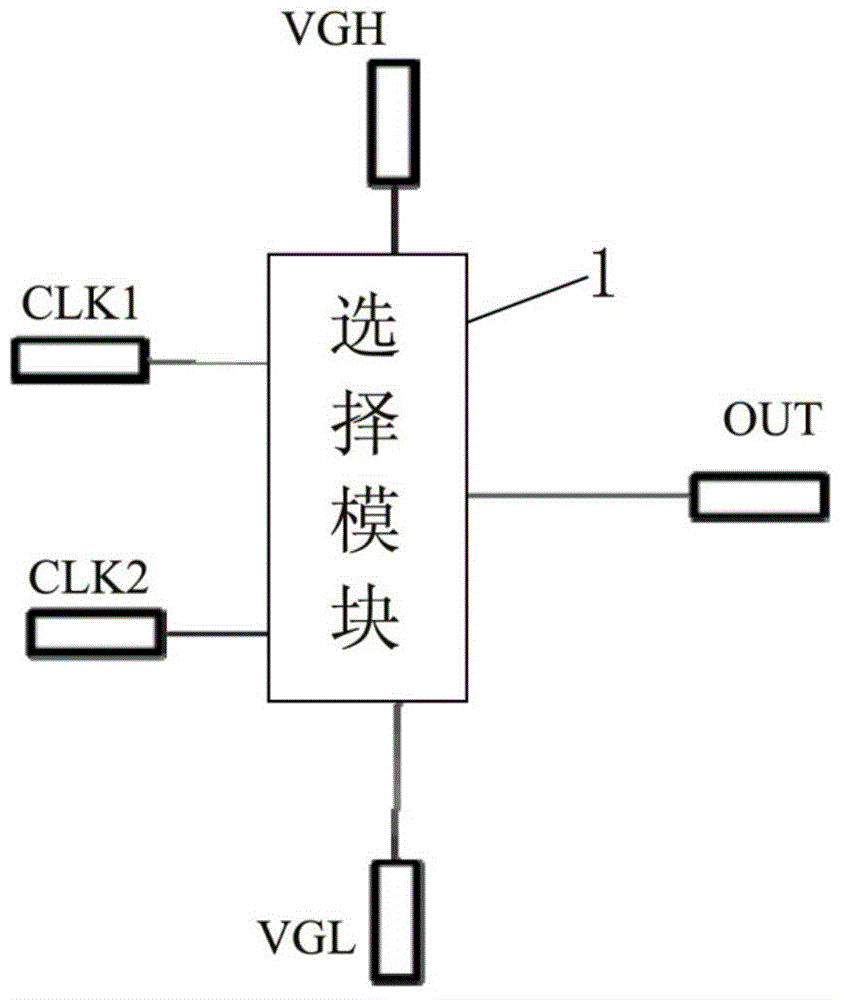
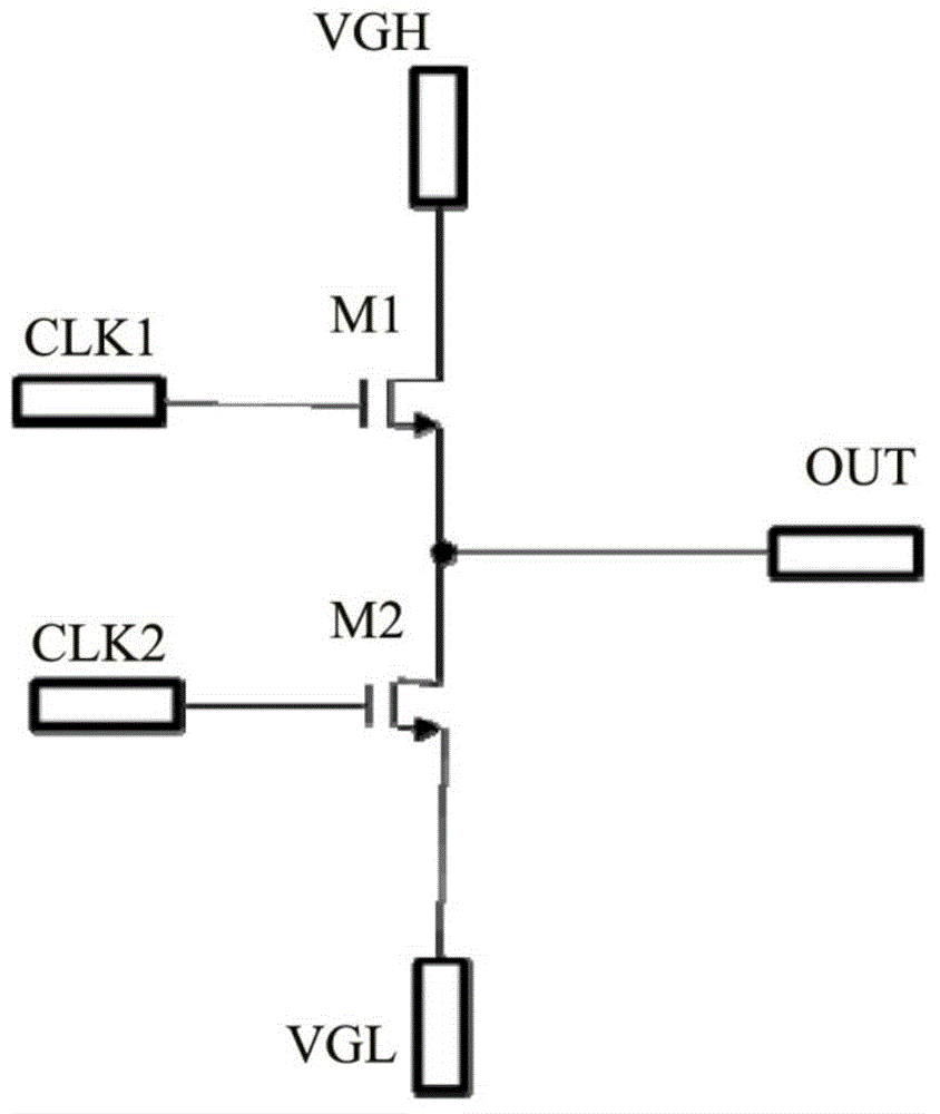
[0030] The present invention provides an implementation manner of a clock signal generation circuit, figure 2 It is a schematic diagram of a clock signal generation circuit provided by an embodiment of the present invention. Such as figure 2 As shown, in this embodiment, the clock signal generating circuit includes a selection module 1, a high-level signal input terminal VGH, a low-level signal input terminal VGL, a first clock signal terminal CLK1, and a second clock signal terminal CLK2, And the output terminal OUT; wherein, the first clock signal terminal CLK1 inputs the first clock signal to the selection module 1; the second clock signal terminal CLK2 i...


PUM


Abstract

The invention relates to a clock signal generation circuit, a grid driving circuit, a display panel and a display device. The clock signal generation circuit comprises a selecting module, a high level signal input end, a low level signal input end, a first clock signal end, a second clock signal end and an output end, wherein the first clock signal end is used for inputting a first clock signal to the selecting module; the second clock signal end is used for inputting a second clock signal to the selecting module; the selecting module is used for gating or disconnecting the high level signal input end with the output end according to the first clock signal, and gating or disconnecting the low level signal input end with the output end according to the second clock signal; the selecting module is also used for gating the high level signal input end and the low level signal input end with the output end in turn and enabling the output end to output a target clock signal. The clock signal generation circuit is capable of reducing distortion of the target clock signal.

Description

technical field [0001] The present invention relates to the field of display technology, in particular to a clock signal generating circuit, a gate driving circuit, a display panel and a display device. Background technique [0002] A thin film transistor liquid crystal display (Thin Film Transistor Liquid Crystal Display, hereinafter referred to as TFT LCD) generally implements display in a progressive scanning manner. The progressive scanning is realized by the gate drive circuit and the source drive circuit; specifically, the gate drive circuit converts the clock signal through the shift register and sequentially loads the clock signal on multiple gate lines of the display panel, thereby driving multiple rows of pixels The thin film transistors are turned on sequentially, and the source drive circuit provides corresponding data signals to each pixel in the turned-on pixel row, so as to realize the display of each row of pixels and the row-by-row display of multiple rows o...

Claims


Application Information

Patent Timeline
Patent Type & Authority Applications(China)
IPC IPC(8): G09G3/36
CPCG06F1/04G09G3/3677G09G2310/0286G09G2310/08G09G2330/06G11C19/287G06F1/06H03K5/135
Inventor 徐飞章祯张志伟
Owner HEFEI BOE OPTOELECTRONICS TECH
Why Eureka
Try Eureka