Printed circuit board and processing method thereof

A technology for printed circuit boards and processing methods, which is applied in the directions of printed circuit, printed circuit manufacturing, and secondary treatment of printed circuit, etc., which can solve the problems that printed circuit boards cannot be increased, and local thick gold positions cannot conduct electricity, so as to provide The effects of production efficiency, shortened processing cycle, and simple operation

Inactive Publication Date: 2015-07-29
SHENZHEN SUNTAK MULTILAYER PCB
View PDF2 Cites 12 Cited by
  • Summary
  • Abstract
  • Description
  • Claims
  • Application Information

AI Technical Summary

Problems solved by technology

[0004] The object of the present invention is to provide a kind of processing method of printed circuit board, by carrying out local electric thickness gold treatment before outer layer etching treatment, aim to solve the problem of partial electric thick gold treatment after outer layer etching treatment in the prior art. The problem that the thick gold position cannot conduct electricity and some printed circuit boards cannot add wires

Method used


Image

  • Printed circuit board and processing method thereof

Examples


Embodiment Construction

[0027] In order to make the object, technical solution and advantages of the present invention clearer, the present invention will be further described in detail below in conjunction with the accompanying drawings and embodiments. It should be understood that the specific embodiments described here are only used to explain the present invention, not to limit the present invention.

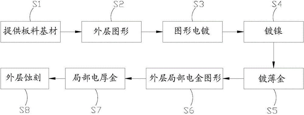
[0028] Please refer to figure 1 , the processing method of the printed wiring board that the embodiment of the present invention provides comprises the following steps:

[0029] S1: Provide a sheet material base material, the sheet material base material includes an inner layer board and a copper foil layer provided on at least one outer surface of the inner layer board, and a layer penetrating through the copper foil layer and the inner layer The conduction hole of the board, the copper foil layer is provided with a local electric gold position, and the hole wall of the conduction hole is formed ...


PUM


Abstract

The invention is applied to the technical field of a printed circuit board, and provides a processing method of a printed circuit board and a printed circuit board formed by use of the processing method, for the purpose of solving the problems that since local electroplating thick gold processing is carried out after external-layer etching processing, a local electroplating thick gold position cannot be conductive and lead wires cannot be added to a part of the printed circuit board in the prior art. The processing method of the printed circuit board comprises the following step of providing a plate substrate, an external-layer pattern, pattern electroplating, nickel plating, thin gold plating, external-layer local electroplating gold pattern processing, the local electroplating thick gold processing and external-layer etching. According to the processing method, before the external-layer etching processing, the external-layer local electroplating gold pattern processing and the local electroplating thick gold processing are carried out, so that conductive lead wires are additionally arranged on an external-layer line pattern, the whole copper foil layer of the plate substrate can be conductive, the membrane removing operation is simple, the manufacturing efficiency is improved, and the processing period is shortened.

Description

technical field [0001] The invention belongs to the technical field of printed circuit boards, and in particular relates to a processing method of a printed circuit board and a printed circuit board formed by the processing method. Background technique [0002] With the continuous upgrading of electronic products, the surface treatment of printed circuit boards is becoming more and more complicated. Usually, multiple surface treatments are required on the same printed circuit board, which makes the processing of printed circuit boards more difficult. [0003] The common surface treatment of printed circuit boards is to adopt the method of thin gold on the whole board and thick gold on some parts. The specific manufacturing process: lamination→outer layer drilling→outer layer copper sinking→full board electroplating→outer layer circuit pattern →Graphic copper plating→nickel plating→thin gold plating→outer layer etching→solder resist→outer layer local electro-gold graphics→loc...

Claims


Application Information

Patent Timeline
Patent Type & Authority Applications(China)
IPC IPC(8): H05K3/00H05K3/24
Inventor 常文智彭卫红王海燕宋建远
Owner SHENZHEN SUNTAK MULTILAYER PCB
Why Eureka
Try Eureka