
Photolithographic illuminator that is telecentric in two directions

A technology of an illuminator and a concentrator, applied in the field of illuminators, can solve the problems of complicated adjustment of the illuminator and increase the sensitivity, etc., and achieve the effect of increasing sharpness and low sensitivity

Inactive Publication Date: 2015-08-05
SAGEM DEFENSE SECURITE SA +1
View PDF4 Cites 1 Cited by
  • Summary
  • Abstract
  • Description
  • Claims
  • Application Information

AI Technical Summary

Problems solved by technology

At this point, the larger aperture limits the depth of field of the microlens array L3, which increases the sensitivity to defocusing of the shutter relative to the object-side focal plane of the array L3
The adjustment of the illuminator thus becomes more complicated

Method used


Image

  • Photolithographic illuminator that is telecentric in two directions
  • Photolithographic illuminator that is telecentric in two directions
  • Photolithographic illuminator that is telecentric in two directions

Examples


Embodiment Construction

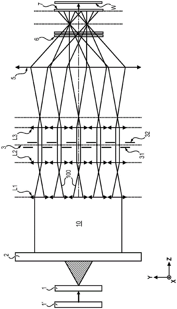
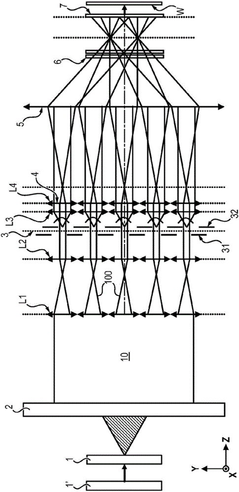
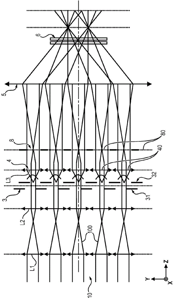
[0050] General description of the illuminator

[0051] Figure 2a , 2b and 2c schematically show a part of an illuminator according to the invention.

[0052] exist Figure 2a In, the illuminator comprises: a light source 1' of a light beam 10, such as a laser light source; a diffractive element 1, which is located at the output of the light source 1'; and a zoomer 2 (these elements are not shown in Figure 2b and Figure 2c middle).

[0053] It further comprises an afocal system L1L2, at the output of the zoomer 2, consisting of a first and a second microlens array L1 and L2.

[0054] Beam 10 comprises a plurality of sub-beams 100 at the output of afocal system L1L2, forming a sub-exit pupil of afocal system L1L2.

[0055] The illuminator comprises a shutter 3, shown as two grids 31, 32, and located at the exit pupil of the afocal system L1L2.

[0056] The light homogenizing system 4 is located downstream of the shutter 3, so that the shutter 3 is located on the object...


PUM


Abstract

The invention relates to a photolithographic illumination device including: a light beam source; a condenser (5); an optical homogenizing system (4), including at least one microlens array (L3, L4), arranged upstream from the condenser (5) such that the image focal plane of the optical homogenizing system is positioned in the object focal plane of the condenser; a shutter (3), arranged in the object focal plane of the optical homogenizing system, and in which the optical homogenizing system includes two microlens arrays (L3, L4), the spacing as well as the arrangement and orientation of the microlenses of which are designed such that, in two directions (X, Y) orthogonal to the optical axis, the optical homogenizing system has merged image focal planes and merged object focal planes. The invention likewise relates to a photolithographic device including such an illuminator.

Description

technical field [0001] The present invention relates to an illuminator of a lithographic apparatus, and to such a lithographic apparatus. Background technique [0002] Photolithography is a technique for manufacturing semiconductor devices by using electromagnetic radiation to create fine patterns on the semiconductor devices. For this purpose, an illuminator of a lithographic apparatus illuminates a mask, the image of which is projected onto a semiconductor wafer (aka "wafer"). [0003] refer to figure 1 , the known illuminator generally comprises a diffractive optical element (also called DOE), which is illuminated by an illumination source 1'. [0004] The radiation source 1' is for example a laser source. [0005] Element 1 may be any element commonly used to generate diffraction, such as a two-dimensional array of spherical microlenses, a Fresnel lens, a diffraction grating, and the like. This element acts as an optical scattering device and has the primary function...

Claims


Application Information

Patent Timeline
Patent Type & Authority Applications(China)
IPC IPC(8): G03F7/20G02B27/09
CPCG02B27/0961G03F7/70066G02B27/0927G03F7/70075G03F7/7015
Inventor B·普兰尚R·梅西耶伊捷
Owner SAGEM DEFENSE SECURITE SA
Features
  • Generate Ideas
  • Intellectual Property
  • Life Sciences
  • Materials
  • Tech Scout
  • Unparalleled Data Quality
  • Higher Quality Content
  • 60% Fewer Hallucinations
Learn More