Semiconductor structure and method for forming same
A semiconductor and substrate technology, applied in the field of semiconductor structure and its formation, can solve problems such as poor glue uniformity, exposure virtualization, abnormal photolithography, etc.
- Summary
- Abstract
- Description
- Claims
- Application Information
AI Technical Summary
Problems solved by technology
Method used
Image

Examples
Embodiment Construction
[0038] In order to make the above objects, features and advantages of the present invention more comprehensible, specific implementations of the present invention will be described in detail below in conjunction with the accompanying drawings.
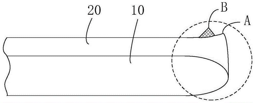
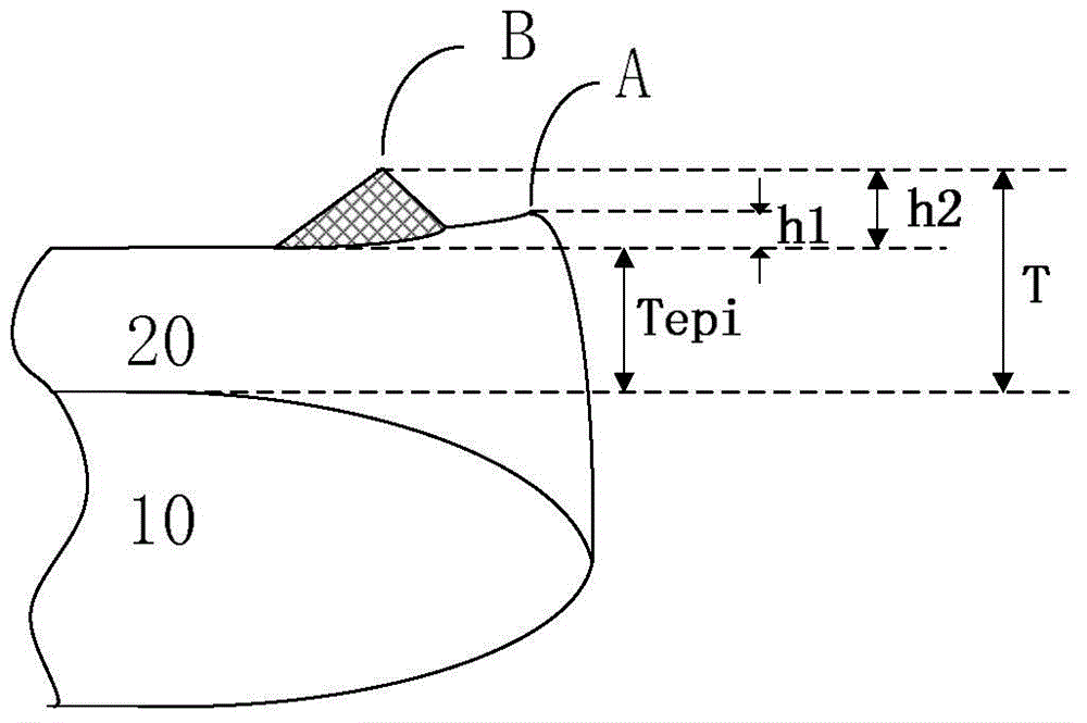
[0039] Such as Figure 8 and Figure 9 As shown, the present invention provides a semiconductor structure, comprising:
[0040] a semiconductor substrate 30 having a single crystal silicon surface;
[0041] A blocking layer 31 formed on the edge region of the semiconductor substrate 30;
[0042] The first epitaxial layer 33a formed in the central region of the semiconductor substrate 30 and the second epitaxial layer 33b formed above the blocking layer 31 are simultaneously formed by an epitaxial growth process.
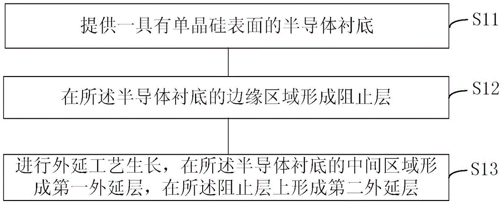
[0043] see image 3 , the present invention also provides a method for forming a semiconductor structure, comprising the steps of:
[0044] S11, providing a semiconductor substrate having a single crystal silicon surface...
PUM
 Abstract
Description
Claims
Application Information
 - R&D
- Intellectual Property
- Life Sciences
- Materials
- Tech Scout
- Unparalleled Data Quality
- Higher Quality Content
- 60% Fewer Hallucinations
Browse by: Latest US Patents, China's latest patents, Technical Efficacy Thesaurus, Application Domain, Technology Topic, Popular Technical Reports.
© 2025 PatSnap. All rights reserved.Legal|Privacy policy|Modern Slavery Act Transparency Statement|Sitemap|About US| Contact US: help@patsnap.com