Conversion circuit from coplanar waveguides to substrate integrated non-radiative dielectric waveguide

A technology of coplanar waveguide and dielectric waveguide, which is applied to circuits, waveguide-type devices, electrical components, etc., can solve problems such as manufacturing and integration difficulties, and achieve the effects of suppressing leakage loss, simple manufacturing process, and reducing circuit volume.

Inactive Publication Date: 2015-08-12
NANJING UNIV OF POSTS & TELECOMM
View PDF7 Cites 4 Cited by
  • Summary
  • Abstract
  • Description
  • Claims
  • Application Information

AI Technical Summary

Problems solved by technology

[0007] In order to overcome the difficulty in making and integrating traditional non-radiative dielectric waveguides, the present invention provides a conversion circuit from coplanar waveguide to substrate integrated non-radiative dielectric waveguide

Method used


Image

  • Conversion circuit from coplanar waveguides to substrate integrated non-radiative dielectric waveguide
  • Conversion circuit from coplanar waveguides to substrate integrated non-radiative dielectric waveguide
  • Conversion circuit from coplanar waveguides to substrate integrated non-radiative dielectric waveguide

Examples


Embodiment Construction

[0019] Below in conjunction with accompanying drawing, technical scheme of the present invention is described in further detail:

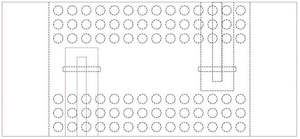
[0020] Such as figure 1 As shown, the overall structure of the present invention from top to bottom is: the first coplanar waveguide, the first dielectric substrate and the first ground plane, the printed circuit board, the second ground plane, the second dielectric substrate and the second coplanar waveguide . Such as figure 2 As shown, the printed circuit board is symmetrically provided with air holes on both sides of the folding line along the long side direction; A rectangular slot; on the second ground plate, a second rectangular slot perpendicular to the metal strip of the second coplanar waveguide is arranged on the fold line along the long side direction.

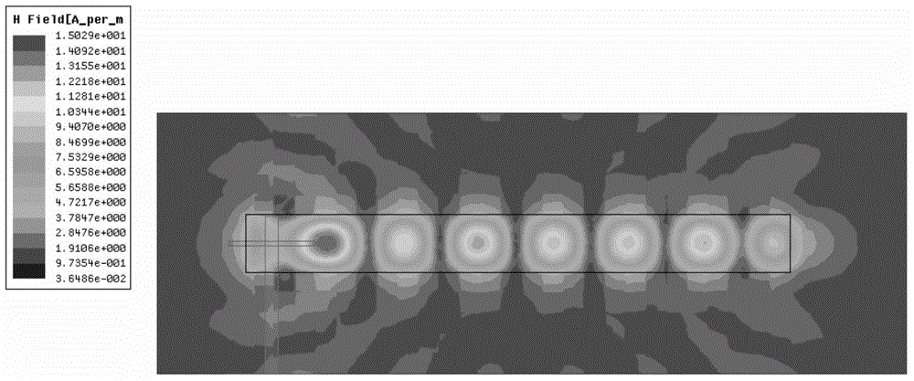
[0021] In terms of circuit function, the present invention has a three-layer circuit structure of a first coplanar waveguide, a substrate-integrated non-radiative dielectric waveguid...


PUM


Abstract

The invention discloses a conversion circuit from coplanar waveguides to a substrate integrated non-radiative dielectric waveguide. The conversion circuit is a dual conversion three-layer circuit structure formed by clamping a layer of substrate integrated non-radiative dielectric waveguide between two layers of coplanar waveguides. By opening a rectangular slot in a grounding plate, an electromagnetic field transmitted in the coplanar waveguide at the top is coupled into the substrate integrated non-radiative dielectric waveguide in the middle, and is then coupled from the substrate integrated non-radiative dielectric waveguide into the coplanar waveguide at the bottom. The substrate integrated non-radiative dielectric waveguide is achieved by designing a series of air through holes in a printed circuit board. According to the invention, the conversion circuit can successfully achieve the transition from a planar structure to a non-planar structure, and facilitate the design and integration of a millimeter-wave frequency band circuit; and is simple in production process and low in cost.

Description

technical field [0001] The invention relates to a conversion circuit from a coplanar waveguide to a substrate integrated non-radiative dielectric waveguide, which belongs to the field of microwave technology. Background technique [0002] With the rapid development of modern wireless communication technology, spectrum resources are increasingly scarce, which makes the research and application of microwave circuits expand to millimeter wave and higher frequency bands. Non-radiative dielectric waveguides have low radiation and leakage losses at structural bends and discontinuities, making them an important component in circuit design at mmWave frequencies. [0003] However, the traditional non-radiative dielectric waveguide has the following two problems when it is applied to millimeter wave circuit design: [0004] 1) The manufacturing process of traditional non-radiative dielectric waveguides is complicated, and the upper and lower metal plates need to be pasted on both sid...

Claims


Application Information

Patent Timeline
Patent Type & Authority Applications(China)
IPC IPC(8): H01P1/16
Inventor 许锋李帆
Owner NANJING UNIV OF POSTS & TELECOMM
Why Eureka
Try Eureka