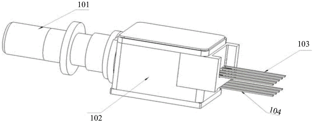
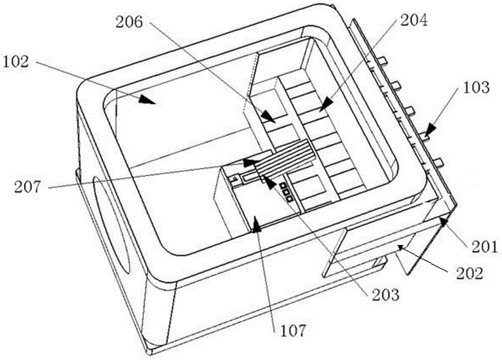
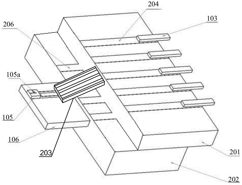
Optical device

An optical device and laser technology, which is applied in the field of optical communication and can solve the problems of the high frequency signal of the input laser being greatly affected.

Active Publication Date: 2015-08-12
HISENSE BROADBAND MULTIMEDIA TECH
View PDF6 Cites 13 Cited by
  • Summary
  • Abstract
  • Description
  • Claims
  • Application Information

AI Technical Summary

Problems solved by technology

Among them, since the external PCB circuit board supplies power to the laser and other components through the conductive path between the PCB board and t

Method used


Image

  • Optical device
  • Optical device
  • Optical device

Examples


Embodiment Construction

[0049] The following will clearly and completely describe the technical solutions in the embodiments of the present invention with reference to the accompanying drawings in the embodiments of the present invention. Obviously, the described embodiments are only some, not all, embodiments of the present invention. Based on the embodiments of the present invention, all other embodiments obtained by persons of ordinary skill in the art without making creative efforts belong to the protection scope of the present invention.

[0050] In describing the present invention, it is to be understood that the terms "center", "upper", "lower", "front", "rear", "left", "right", "vertical", "horizontal", The orientations or positional relationships indicated by "top", "bottom", "inner", "outer", etc. are based on the orientations or positional relationships shown in the drawings, and are only for the convenience of describing the present invention and simplifying the description, rather than in...


PUM


Abstract

The embodiment of the present invention provides an optical device which relates to the optical communication field, and can satisfy the impedance matching requirement of the high frequency signal transmission. The optical device comprises a first substrate, a second substrate and a transfer plate, a first conductive access is arranged on the upper surface of the first substrate, a second conductive access is arranged on the lower surface of the first substrate, and a third conductive access is arranged on the upper surface of the second substrate. A microstrip line structure is arranged on the transfer plate and comprises a transfer line arranged on the upper surface of the transfer plate, and the upper surface of the second substrate is opposite to the lower surface of the first substrate, wherein the second conductive access is attached to the third conductive access, and the transfer plate is arranged above the upper surface of the second substrate and is located in the third conductive access. One end of the transfer line is electrically connected with the first conductive access by threading, and the other end is connected with an internal element in the optical device by threading. The embodiment of the present is used for the optical device manufacture.

Description

technical field [0001] The invention relates to the field of optical communication, in particular to an optical device. Background technique [0002] The development of optical modules and optical devices in the field of optical communication is very rapid. With the construction of a large number of FTTH (Fiber To The Home, fiber directly to the home) and 3G / 4G networks in China, the demand for optical modules and optical devices is increasing. Therefore, optical modules and optical devices with high development speed, long transmission distance, miniaturization and low power consumption have become the focus of equipment manufacturers and device manufacturers. [0003] Among them, in order to adapt to the miniaturization of optical devices, packaged lasers and other electrical devices are usually used as optical devices, and the lasers and other electrical devices packaged inside are connected to the external PCB (Printed Circuit Board, printed circuit board) circuit board ...

Claims


Application Information

Patent Timeline
IPC IPC(8): H04B10/25
CPCH01S5/02469H01S5/06226G02B6/4269G02B6/4292H01P3/081H01L2224/45144H01L2224/48227H01S5/02345H01L2924/00014H01S5/0687H01S5/06837H01S5/068H01S5/02407H01S5/02415H01S5/024H01L24/00H01L23/00G02B6/4278G02B6/4279
Inventor 王昊穆洪伟黄永亮张舜
Owner HISENSE BROADBAND MULTIMEDIA TECH
Why Eureka
Try Eureka