
semiconductor storage device

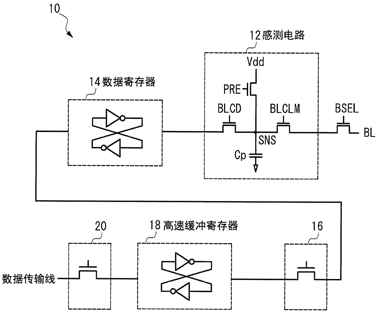
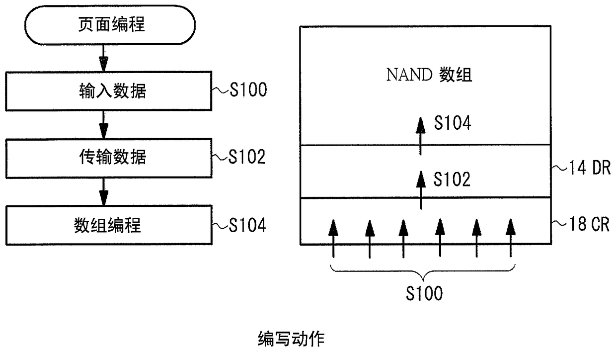
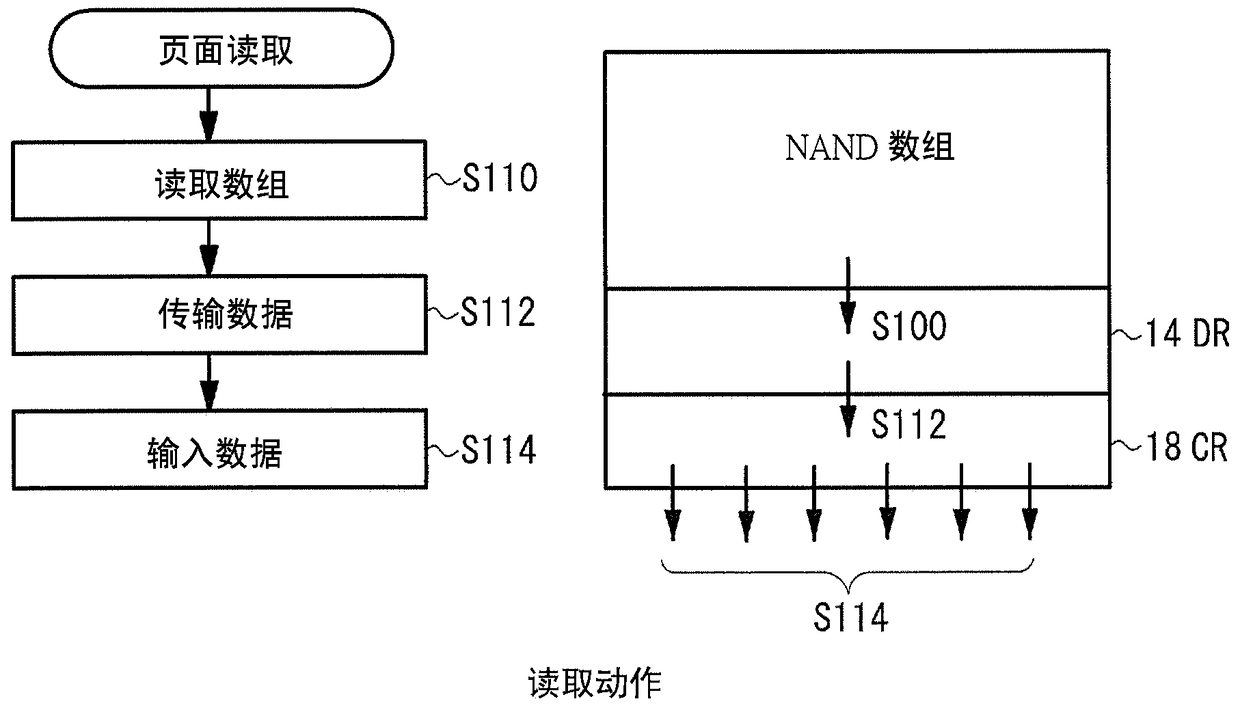
A storage device and semiconductor technology, which is applied in the field of page buffers, can solve the problems of data disappearance, inability to program the entire page, and larger occupied area, etc., and achieve the effect of high-speed, flexible reading and writing actions

Active Publication Date: 2019-01-08
WINBOND ELECTRONICS CORP
View PDF4 Cites 0 Cited by
  • Summary
  • Abstract
  • Description
  • Claims
  • Application Information

AI Technical Summary

Problems solved by technology

[0011] First, if the page buffer is configured with a CMOS latch circuit, etc., the area occupied will increase, and as a result, the miniaturization of the flash memory cannot be achieved.
[0012] Second, because the page buffer is volatile, the data disappears if power is removed
In other words, it means that in the case of data smaller than 512 bytes, even if the same page is programmed continuously, the entire page cannot be programmed

Method used


Image

  • semiconductor storage device
  • semiconductor storage device
  • semiconductor storage device

Examples


Embodiment

[0074] image 3 It is a block diagram showing the structure of a flash memory according to an embodiment of the present invention. However, the configuration shown here is an example, and the flash memory of the present invention is not necessarily limited to this configuration.

[0075] The flash memory 100 of this embodiment is configured to include: a storage array 110, which forms a plurality of storage cells arranged in a matrix; an input and output buffer 120, which is connected to an external input and output terminal I / O and holds input and output data; and an address register 130. Receive address data from the input and output buffer 120; the controller 140, according to the command data from the input and output buffer 120 and an external control signal not shown (Command latch enable (CLE) signal or The address latch enable (ALE) signal, etc.) are used to control each part; the word line selection circuit 150 decodes the row address information Ax from the address regi...


PUM


Abstract

The invention provides a semiconductor storing device. A flash memory of the invention comprises a page buffer or a sensing circuit and a high-speed buffer register. The page buffer or sensing circuit comprises a volatile storage element of data capable of keeping the size corresponding to the page of a storage array. The high-speed buffer register comprises a nonvolatile storage element of the data capable of keeping the size corresponding to the page of the storage array. The page buffer or sensing circuit comprises a sensing circuit, a data register and a transmission grid. Data transmission and receiving can be performed between the data register and an input-output buffer. The high-speed buffer register comprises a resistive random access memory (RRAM). The RRAM can receive or transmit data from or to the input-output buffer through the transmission grid. The RRAM also can receive or transmit data from or to the data register through the transmission grid.

Description

Technical field [0001] The present invention relates to a semiconductor storage device such as a NAND flash memory, and more particularly to a page buffer using non-volatile memory. Background technique [0002] As we all know, NAND-type flash memory includes: a memory cell array, which includes a NAND string formed by connecting a plurality of memory cells in series; and a page buffer, which is connected to a bit line of the memory array. The page buffer holds the data transferred from the selected page of the storage array, or holds the data written to the selected page. A flash memory is disclosed, in which the page buffer includes a data register and a cache register to achieve high-speed reading and writing (Patent Document 1). [0003] [Background Technical Literature] [0004] [Patent Literature] [0005] [Patent Document 1] Japanese Patent Laid-Open No. 2013-118031 [0006] In the conventional NAND-type flash memory, the page buffer that holds the page data read from the memo...

Claims


Application Information

Patent Timeline
Patent Type & Authority Patents(China)
IPC IPC(8): G11C16/06G11C16/26
Inventor 妹尾真言
Owner WINBOND ELECTRONICS CORP
Learn More