Automatic etching and cleaning device for PCB

A technology for PCB boards and cleaning devices, which is applied in the cleaning/polishing of conductive patterns, secondary processing of printed circuits, electrical components, etc., can solve the problems of high labor intensity, worker hazards, corrosion of etching liquid, etc., and reduce labor intensity. , High degree of automation, ensure the effect of cleaning quality

Inactive Publication Date: 2015-08-19
CHENGDU HONGHUA ENVIRONMENTAL SCI & TECH CO LTD
View PDF4 Cites 6 Cited by
  • Summary
  • Abstract
  • Description
  • Claims
  • Application Information

AI Technical Summary

Problems solved by technology

[0002] With the recovery of the electronics industry, the development of China's circuit board industry has also generally rebounded. China will become the world's largest PCB industry base in recent years, accounting for about 30% of the global market. In the production process of printed circuit boards, etching is It is a very important process, and a large amount of etching solution must be used during etching. However, the existing etching equipment is not highly automated and often requires manual operation. However, the etching solution is highly corrosive and is likely to cause harm to workers. Moreover, as the etching progresses, the copp

Method used


Image

  • Automatic etching and cleaning device for PCB
  • Automatic etching and cleaning device for PCB
  • Automatic etching and cleaning device for PCB

Examples


Embodiment Construction

[0013] The present invention will be further described below in conjunction with accompanying drawing, protection scope of the present invention is not limited to the following:

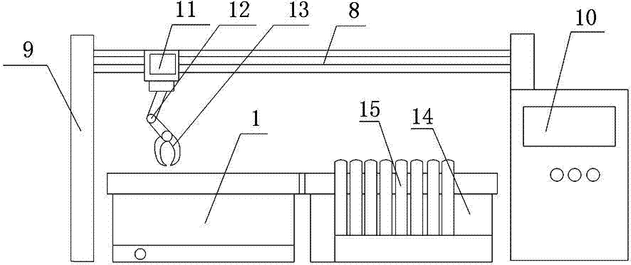
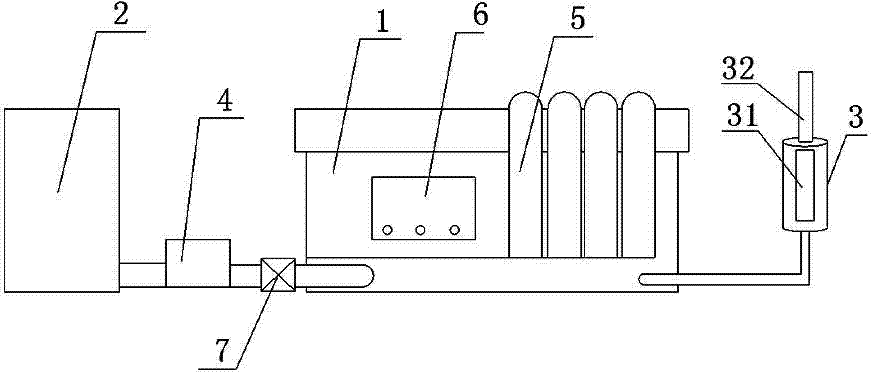
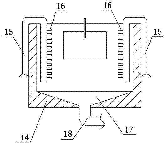
[0014] Such as figure 1 Shown, a kind of PCB board automatic etching cleaning device, it comprises etching tank 1, cleaning tank 14, grasping mechanism, cross bar 8, support 9 and control box 10, described grasping mechanism comprises manipulator controller 11, mechanical Arm 12 and manipulator 13, described manipulator controller 11 and manipulator 12 are flexibly connected, and lead wire is connected between manipulator controller 11 and manipulator 13, and manipulator controller 11 is movably installed on cross bar 8, and described cross bar 8 is installed on the bracket 9, and the control box 10 is connected with the manipulator controller 11. In this embodiment, the control box 10 controls the manipulator 13 to move laterally, and the manipulator controller 11 controls the manipulator 13 to grab...


PUM

PropertyMeasurementUnit
Rotation angleaaaaaaaaaa

Abstract

The invention discloses an automatic etching and cleaning device for a PCB, and the device comprises an etching tank, a cleaning tank, a grabbing mechanism, a cross bar, a support, and a control box. The grabbing mechanism comprises a mechanical arm controller, a mechanical arm, and a mechanical hand. The etching tank is provided with an etching agent tube, and the inlet of the etching agent tube is connected with an etching pump. The outlet of the etching agent tube is located in the etching tank, and the etching pump is connected with an etching auxiliary tank. The interior of a detection apparatus is provided with an aerometer and a probe. A side wall of the etching tank is provided with a controller, and two side walls of the cleaning tank are respectively provided with a plurality of tap water pipes. The outlets of the plurality of tap water pipes are located in the cleaning tank, and are sequentially provided with a plurality of high-pressure spraying heads from the top to the bottom. The bottom of the cleaning tank is provided with a tapered tank, and the bottom of the tapered tank is provided with a water outlet pipe. The beneficial effects of the invention are that the device is high in automation degree, is good in etching quality, and is good in cleaning quality.

Description

technical field [0001] The invention relates to an etching cleaning device, in particular to an automatic etching cleaning device for a PCB board. Background technique [0002] With the recovery of the electronics industry, the development of China's circuit board industry has also generally rebounded. China will become the world's largest PCB industry base in recent years, accounting for about 30% of the global market. In the production process of printed circuit boards, etching is It is a very important process, and a large amount of etching solution must be used during etching. However, the existing etching equipment is not highly automated and often requires manual operation. However, the etching solution is highly corrosive and is likely to cause harm to workers. Moreover, as the etching progresses, copper is continuously dissolved, and the content of monovalent copper ions in the potion rises, which means that divalent copper ions in the etching solution need to be con...

Claims


Application Information

Patent Timeline
IPC IPC(8): H05K3/26
CPCH05K3/26H05K2203/075H05K2203/0766
Inventor 韦建敏赵兴文张晓蓓张小波
Owner CHENGDU HONGHUA ENVIRONMENTAL SCI & TECH CO LTD
Why Eureka
Try Eureka