Inorganic barrier layers

A technology of exciton blocking layer and inorganic materials, which can be used in organic semiconductor devices, radiotherapy, treatment, etc., and can solve problems such as unsatisfactory device efficiency

Inactive Publication Date: 2015-08-19
MERCK PATENT GMBH
View PDF13 Cites 1 Cited by
  • Summary
  • Abstract
  • Description
  • Claims
  • Application Information

AI Technical Summary

Problems solved by technology

[0013] However, the efficiency of said devices emitting UV radiation in the UV region is still not satisfactory

Method used


Image

  • Inorganic barrier layers
  • Inorganic barrier layers
  • Inorganic barrier layers

Examples


Embodiment 1

[0134] Material

[0135] The following two emitters E1 and E2 are used.

[0136]

[0137] The synthesis of E1 is disclosed in EP 329752 and the synthesis of E2 in EP 440082.

[0138] The host used was polystyrene (PS) from Fluka (81414, Mw 500000, Mn 490000). BM1 and BM2 are ZrO x and HfO x precursor material (x≤2). The synthesis of the precursors was performed according to WO 2010 / 078907.

Embodiment 2

[0140] Solutions and compositions comprising matrix material and emitter

[0141] Solutions as outlined in Table 1 were prepared as follows: First, the host and emitter mixture was dissolved in 10 ml toluene and stirred until the solution was clear. The solution was filtered using a Millipore Millex LS hydrophobic PTFE 5.0 μm filter.

[0142] Table 1:

[0143]

[0144] These solutions are used to make the emissive layers of OLEDs. The corresponding solid compositions can be obtained by evaporating the solvent from the solutions. This can be used to prepare additional formulations.

Embodiment 3

[0146] Fabrication of organic electroluminescent devices

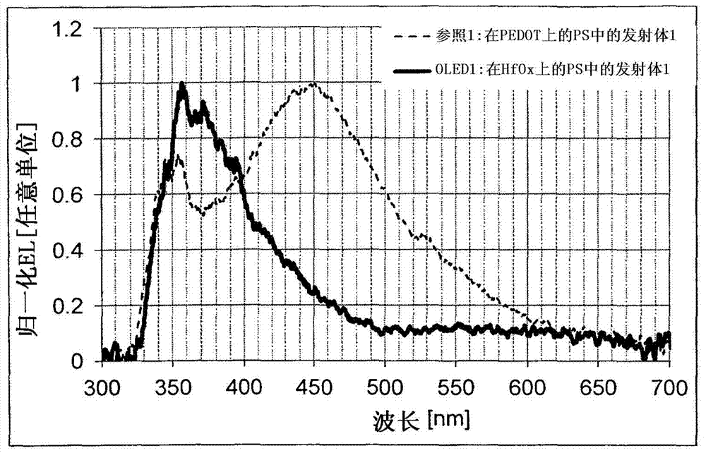
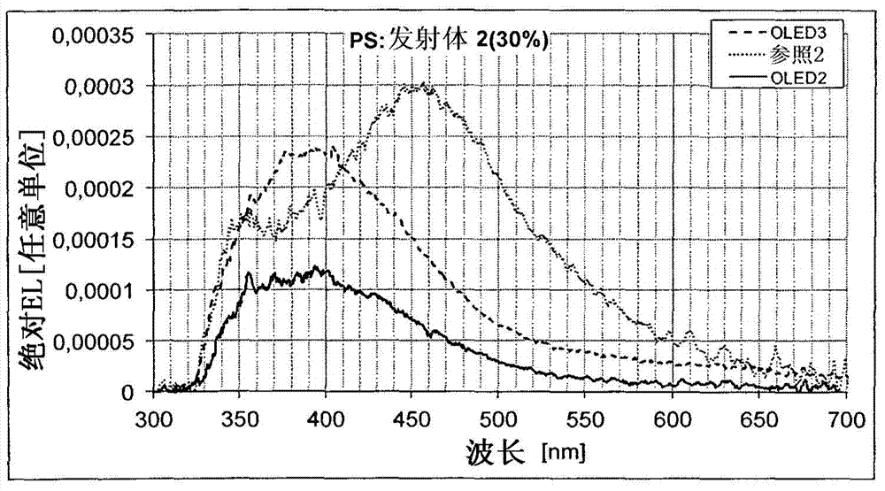
[0147] OLED Reference 1 and Reference 2 have the following structure: ITO / PEDOT / EML / cathode. These two OLEDs were used as reference examples. They were produced according to the following steps using the corresponding solutions from Table 1:

[0148] 1. 80nm PEDOT (Clevios TM P VP AI 4083) was applied to an ITO-coated glass substrate. It was then dried by heating at 120° C. for 10 minutes in a clean room.

[0149] 2. Apply a 100 nm emissive layer by spin coating the solutions according to Table 1 in an Ar glove box.

[0150] 3. Dry the device by heating at 180°C for 10 minutes.

[0151] 4. Apply Ba / Al cathode (3nm+150nm) by vapor deposition.

[0152] 5. Package the device.

[0153]OLED1-OLED3 are devices according to the invention having the following structure: ITO / BL / EML / cathode, where BL stands for exciton blocking layer. They were produced using the solutions from Table 1 by the method described for OLED-Re...


PUM


Abstract

The present invention relates to electroluminescent devices containing materials having a wide band gap and to the use thereof.

Description

technical field [0001] The invention relates to organic electroluminescent devices comprising inorganic barrier layers and their use. Background technique [0002] Structures of organic electroluminescent devices (for example organic light-emitting diodes—OLEDs) in which organic semiconductors are used as functional materials are described, for example, in US 4539507, US 5151629, EP 0676461 and WO 98 / 27136. In addition to fluorescent emitters, the emissive materials used here are increasingly organometallic complexes, which exhibit phosphorescence (M.A. Baldo et al., Appl. Phys. Lett. (Applied Physics Letters) 1999,75,4 ~6). For quantum mechanical reasons, up to four times higher energy and power efficiencies can be achieved using organometallic compounds as phosphorescent emitters. In general, in the case of OLEDs exhibiting singlet emission as well as in the case of OLEDs exhibiting triplet emission, improvements are still required, especially with regard to efficiency, ...

Claims


Application Information

Patent Timeline
Patent Type & Authority Applications(China)
IPC IPC(8): H01L51/50H01L51/52
CPCH01L51/5096H01L51/52H10K50/18H10K50/80H10K71/00H10K50/11H10K50/13H10K50/16H10K50/81H10K50/82H10K50/171H10K85/60H10K85/111H10K2102/00A61N5/0616A61N2005/0653A61N2005/0661
Inventor 潘君友安德里亚斯·克吕什奇
Owner MERCK PATENT GMBH
Why Eureka
Try Eureka